For contact info, please see the Sci.Electronics.Repair FAQ Email Links Page.
Copyright © 1994-2024
Reproduction of this document in whole or in part is permitted if both of the
following conditions are satisfied:
1.This notice is included in its entirety at the beginning.
We will not be responsible for damage to equipment, your ego, county wide
power outages, spontaneously generated mini (or larger) black holes, planetary
disruptions, or personal injury or worse that may result from the use of this
material.
Perhaps the larges collection of all sorts of on-line schematics and links
in the explored universe can be found Tomi Engdahl's
Lights and
Electronics Page.
There are many other documents at the
Sci.Electronics.Repair (S.E.R) FAQWeb
site or one of its mirror sites which may be of use in the design, testing, and
repair of electronic equipment. The
Main Table of Contents (ToC)
provides links to a variety of information on troubleshooting and repair of
many types of equipment, general electronics, an assortment of schematics,
over 1,000 technology links, and much more. Most of these documents are nicely
formatted, indexed, and cross-referenced. (Silicon Sam's
Technology Resource, which may be present at this site and others, usually
contains slightly more recent versions of many of these same documents but most
of those under the S.E.R FAQ Main ToC are easier to use and the actual content
differences are likely to be minor.)
The input voltage can range from about 5 to 24 V. Using a flyback from a MAC
Plus computer which had its bad primary winding excised, an output of more than
20 kV was possible (though risky since the flyback is probably not rated for
more than about 12 kV) from a 24 VDC, 2 A power supply. By adjusting the drive
frequency and duty cycle, a wide range of output voltages and currents may
be obtained depending on your load.
With the addition of a high voltage filter capacitor (0.08 uF, 12 kV), this
becomes a nice little helium neon laser power supply which operates on 8 to
15 VDC depending on required tube current and ballast resistor. See the
document: Sam's Laser
FAQ.
The transistor types are not critical. Those were selected basically because
I had them in my junk box. A TV or monitor horizontal output transistor (HOT)
should be satisfactory for the chopper but will require good strong drive.
The lower voltage, high current transistor I used (2SD797) has both a higher
current and higher Hfe rating than typical HOTs. Even a 2N3055 will probably
survive and not be too bad in the performance department.
The drive transformer is from a B/W computer monitor (actually a video display
terminal) and has a turns ratio of 4:1 wound on a 5/16" square by 3/8" long
nylon bobbin on a gapped ferrite double E core. The primary has 80 turns and
the secondary has 20 turns, both of #30 wire. Make sure you get the polarity
correct: The base of the switching transistor should be driven when the driver
turns on. You should be able to wind a transformer similar to this in about
10 minutes if a similar size (doesn't need to be exact) core is available.
Where the flyback includes an internal rectifier and/or you are attempting
to obtain the maximum output voltage of a specific polarity, the direction of
drive matters as the largest pulse amplitude is generated when the switching
transistor turns off. Since flyback transformers are not marked, you will
have to try both possible connections to the drive coil. Use the one that
produces the higher output voltage for a given set of input conditions (drive
and pulse rate/width).
Many variations on this basic circuit are certainly possible. The dual 555
circuit can be reduced to a single 555 with some loss in flexibility (unless
you use the cute non-standard modification that allow independent adjustment
of the high and low times - left as an exercise for the student).
One nice thing about running it at 24 VDC or less (as opposed to line
voltage) is that it is much more difficult to let the smoke out of th
circuit! The 5 A power supply I was using shut down on several occasions
due to overcurrent but the only time I blew the chopper transistor was by
accidentally shorting the base to collector.
Evertron Model 3210 Gas Tube Power Supply is
the schematic of an inverter type unit for driving a neon sign. It has a pair
of power MOSFETs driving a flyback style high voltage transformer, with a
whole bunch of open-wound primaries and a potted secondary.
The adjustments on each section are for the current limit, not output voltage
as might be expected. The output voltage for each section is set by fixed
resistors (one of which is inside the potted HV module).
It would be a simple matter to replace R12 or R32 to vary the C or T
output voltages within a modest range (like 4 to 6 kV). But going
too high is asking for smoke. :) If pots are used, make sure their
maximum value will limit the output voltage to something reasonable.
Many modern gas stoves, ovens, furnaces, and other similar appliances use an
electronic ignition rather than a continuously burning pilot flame to ignite
the fuel. These are actually simple high voltage pulse generators.
The high-tech versions consist of a high voltage low current power supply and
fluorescent (usually) lamp selected to attract undesirable flying creatures.
(Boring low-tech devices may just use a fan to direct the insects to a tray of
water from which they are too stupid to be able to excape!)
However, these devices are not selective and will obliterate friendly and
useful bugs as well as unwanted pests.
Here is a typical circuit:
(From: Andrew Bowers (falcon_@geocities.com).)
This is from my friend's bug zapper:
This is your ultimate simple bug zapper -- no power switch, although the
metal plate that the transformer and other parts are mounted on is grounded.
This module produces both positive and negative outputs when connected to 115
VAC, 60 Hz line voltage. Each is about 5 kV at up to around 5 uA. It is
probably similar to the high voltage power supply in the AirEase(tm) Personal
Space Ionization Air Cleaner from Ion Systems, Inc., a small table top unit.
(Unfortunately, the HV module in the AirEase was totally potted so I could not
determine anything about its internal circuitry.)
The LED (IL1) is a power-on indicator. :-)
The transformer was totally potted so I could not easily determine anything
about its construction other than its winding resistances and turns ratio
(about 1:100).
From my measurements, this circuit produces a total of around 10 kV between
HV+ and HV-, at up to 5 uA. The output voltages are roughly equal plus and
minus when referenced to point B.
I assume the module would also operate on DC (say, 110 to 150 V) with the
discharges repeating continuously at about 2 kHz. Output current capability
would be about 5 times greater but at the same maximum (no load) voltage.
(However, with DC, if the SCR ever got stuck in an 'on' state, it would be
stuck there since there would be no AC zero crossings to force it off. This
wouldn't be good!)
The secondary side circuitry can be easily modified or redesigned to provide
a single positive or negative output or for higher or lower total voltage.
Simply removing R4 will isolate it from the input and earth ground (assuming
T1's insulation is adequate).
Where there is no high voltage from such a device, check the following:
DL1 to DL4 look like neon light bulbs with a single electrode. They glow like
neon light bulbs when the circuit is powered and seem to capacitively couple
the HV pulses to the grounded grid in such a way to generate ozone. I don't
know if they are filled with special gas or are just weird neon light bulbs.
An ultrasonic cleaner contains a power oscillator driving a large piezoelectric
transducer under the cleaning tank. Depending on capacity, these can be quite
massive.
A typical circuit is shown below. This is from a Branson Model 41-4000 which
is typical of a small consumer grade unit. The H and N are Hot and Neutral
of the 115 VAC line. WARNING: Line connected input. Use isolation
transformer for safety when troubleshooting.
The power transistor (Q1) and its associated components form an self excited
driver for the piezo-transducer (PT1). I do not have specs on Q1 but based on
the circuit, it probably has a Vceo rating of at least 500 V and power rating
of at least 50 W.
Two windings on the transformer (T1, which is wound on a toroidal ferrite
core) provide drive (D) and feedback (F) respectively. L1 along with the
inherent capacitance of PT1 tunes the output circuit for maximum amplitude.
The output of this (and similar units) are bursts of high frequency (10s to
100s of kHz) acoustic waves at a 60 Hz repetition rate. The characteristic
sound these ultrasonic cleaners make during operation is due to the effects
of the bursts occuring at 60 Hz since you cannot actually hear the ultrasonic
frequencies they use.
The frequency of the ultrasound is approximately 80 kHz for this unit with a
maximum amplitude of about 460 VAC RMS (1,300 V p-p) for a 115 VAC input.
WARNING: Do not run the device with an empty tank since it expects to have
a proper load. Do not touch the bottom of the tank and avoid putting your
paws into the cleaning solution while the power is on. I don't know what,
if any, long term effects there may be but it isn't worth taking chances.
The effects definitely feel strange. At high enough power levels, it could
indeed pulverize bones as described below. Whether that could happen with
the typical small ultrasonic cleaner, I don't know and am not about to find
out!
(From: BIll Perry (perry.williamr@tacamo.navy.mil).)
"While stationed on board the now-decommissioned submarine USS
Hawkbill (SSN-666), I pondered this as well. One of my senior shipmates
related a story of a sailor who had done that very act on his previous
submarine. The guy put his feet it the cleaner while it was powered on.
He remarked that it felt very good and relaxing. After a few minutes, he
pulled his feet out, and as soon as he stood up and applied his full bodily
weight on his feet, all the bones in his feet had shattered. He got
permanent disability from it. Apparently, it had rattled his bones apart.
Wow!"
Where the device doesn't oscillate (it appears as dead as a door-nail), first
check for obvious failures such as bad connections and cracked, scorched, or
obliterated parts.
To get inside probably requires removing the bottom cover (after pulling the
plug and disposing of the cleaning solution!).
CAUTION: Confirm that all large capacitors are discharged before touching
anything inside!
The semiconductors (Q1, D1, D2, D3) can be tested for shorts with a multimeter
(see the document:
Basic Testing of
Semiconductor Devices.
The transformer (T1) or inductor (L1) could have internal short circuits
preventing proper operation and/or blowing other parts due to excessive load
but this isn't kind of failure likely as you might think. However, where all
the other parts test good but the cleaning action appears weak without any
overheating, a L1 could be defective (open or other bad connections) detuning
the output circuit.
Where the transistor and/or fuse has blown, look for a visible burn mark on
the transducer and/or test it (after disconnecting) with a multimeter. If
there is a mark or your test shows anything less than infinite resistance,
there may have been punch-through of the dielectric between the two plates.
I don't know whether this could be caused by running the unit with nothing in
the tank but it might be possible. If the damage is localized, you may be able
to isolate the area of the hole by removing the metal electrode layer
surrounding it to provide an insulating region 1/4 inch in diameter. This
will change the resonant frequency of the output circuit a small amount but
hopefully not enough to matter. You have nothing to lose since replacing the
transducer is likely not worth it (and perhaps not even possible since it is
probably solidly bonded to the bottom of the tank).
When testing, use a series light bulb to prevent the power transistor from
blowing should there be a short circuit somewhere (see the document:
Troubleshooting and
Repair of Consumer Electronic Equipment) AND do not run the unit with and
empty tank.
Also see the info on ultraonic humidifiers in the document:
Troubleshooting and Repair of Small Household
Appliances.
This is also the simplest and safest way to construct a small DC power supply
as you do not need to deal with the 110 VAC at all.
To convert such an adapter to DC requires the use of:
The basic circuit is shown below:
Therefore, you will need to find an AC wall adapter that produces an output
voltage which will result in something close to what you need. However,
this may be a bit more difficult than it sounds since the nameplate rating
of many wall adapters is not an accurate indication of what they actually
produce especially when lightly loaded. Measuring the output is best.
The following is a very basic introduction to the construction of a circuit
with appropriate modifications will work for outputs in the range of about
1.25 to 35 V and currents up 1 A. This can also be used as the basis for a
small general purpose power supply for use with electronics experiments.
What you want is an IC called an 'adjustable voltage regulator'. The LM317 is
one example - Radio Shack should have it along with a schematic. The LM317
looks like a power transistor but is a complete regulator on a chip.
Here is a sample circuit:
Here are pinouts for the most common types:
Note: Various manufacturers may label the pins differently than shown just to
be confusing. For example, 1,3,2 instead of 1,2,3. However, the location of
each pin will be the same so double check with the diagram.
For the LM317:
However, note that a typical adapter's voltage may vary quite a bit
depending on manufacturer and load. You will have to select one that
isn't too much greater than what you really want since this will add
unnecessary wasted power in the device and additional heat dissipation.
Using 10,000 uF per *amp* of output current will result in less than 1 V
p-p ripple on the input to the regulator. As long as the input is always
greater than your desired output voltage plus 2.5 V, the regulator will
totally remove this ripple resulting in a constant DC output independent
of line voltage and load current fluctuations. (For you purists, the
regulator isn't quite perfect but is good enough for most applications.)
Make sure you select a capacitor with a voltage rating at least 25% greater
than the adapter's *unloaded* peak output voltage and observe the polarity!
Note: wall adapters designed as battery chargers may not have any filter
capacitors so this will definitely be needed with this type. Quick check:
If the voltage on the adapter's output drops to zero as soon as it is pulled
from the wall - even with no load - it does not have a filter capacitor.
For an unregulated supply, take the outputs from V+ and V-.
Here is a circuit for a +/- 12 VDC supply:
Since only half-wave rectification is used, the main filter caps, C1 and C2,
should be at least twice the uF value compared to full wave or bridge circuits
to obtain the same ripple.
Another disadvantage of this configuration is that if the currents drawn from
the outputs aren't equal, net DC flows through the transformer secondary
(with a voltage doubler having no output connection to the common point,
this isn't possible). Core saturation may result if operating near the
transformer's maximum current ratings.
For a negative supply based on a 79xx regulator, use an NPN transistor like
a 2N3055 and reverse the capacitor polarities. Don't forget that the pinout
for the 79xx and other negative voltage regulators is NOT the same as for
the positive variety. See the section: Adding an IC
Regulator to a Wall Adapter or Battery.
* For proper regulation, RL must be low enough in value to guarantee at least a
30 mA current at the selected output voltage. It can be a separate resistor
or part of the actual load.
For even higher current operation, multiple power transistors (Q2) can be
wired in parallel as a pass-bank with small (e.g., 0.1 ohm) emitter resistors
to balance the load. In this case, Q1 may need to be a slightly bigger
transistor and R4 reduced in value to provide adequate base drive. Details
will depend on your particular needs.
As with the other circuits, a negative power supply can be constructed by
using the appropriate regulator IC, swapping NPN or PNP transistors, and
reversing all the polarities of the capacitors and diode.
(From: David Subert (voodoo2daddy@yahoo.com).)
As it turns out, the bipolar transistors can be replaced by IRF9630 MOSFETS.
The only other modification required is to change the value of the 5 ohm
resistor in order to properly bias the MOSFET. This is significant because
MOSFETs can be easily arranged in parallel without having to worry about the
inconsistent BETA of parallel BJTs.
D1 to D4 can be individual diodes or a bridge rated for at least 3 A.
The regulator (IC1) is an LT1084CP which is similar to an LM317 but is a low
dropout type rated at 5 A max. I had a pile of these left over from a certain
multi-million dollar project that had been cancelled due to upper management
foot in a** disease..... An external pass transistor may be needed to use
an LM317 because of the peak current requirement.
Despite the transformer only being rated for 1 A, with IC1 on a modest
heatsink, the supply seems perfectly happy putting out 3 A at 1.5 V for an
extended period. I don't know that I would run it all day at this high
current but for my purposes, it seems fine.
It turns out that the typical electronic flash circuit from a disposable
camera like the Kodak MAX (see Schematic and
Photo), actually draws more
than 3 A at the start of its recharge cycle. So, the voltage does dip a
bit but this doesn't affect much of anything. Recharge time with the power
supply is at least as rapid as with a fresh Alkaline cell. The voltage from
an Alkaline cell also dips a bit under these conditions.
Obviously, the circuit could be easily modified to put out 2.4 VDC (for a pair
of NiCd cells), 3 VDC (for two Alkalines), or whatever else you might need.
Here is a cute circuit that gets around both these problems. The original
article can be found at
Tech Corner
by George Hrischenko VE3DXG.
The output voltage is approximately 2.8 times the RMS rating of the
transformer secondary (primary not shown). Ripple is at 2X the power
line frequency.
Obviously, other voltages than +12 VDC can be produced in this manner - the
example was a coincidence.
This could also be done with fewer components using modern SMPS ICs designed
DC-DC converter applications but I don't have any suggestions off-hand.
Errors in transcription are possible. Some models use additional outputs each
fed from a single rectifier diode and filter capacitor (not shown). Some part
numbers and the connector pinout may not be the same for your particular VCR.
A totally dead supply with a blown fuse usually means a shorted switchmode
power transistor, Q1. Check all other components before applying power
after replacement as other parts may be bad as well.
The most common problems resulting in low or incorrect outputs are dried
up or leaky electrolytic capacitors - C4, C16, C17, C21.
See the document:
Notes on the
Troubleshooting and Repair of Small Switchmode Power Supplies for more
info.
The AC line input and degauss components are at the upper left, the SMPS
chopper, its controller, and feedback opto-isolator are in the lower
left/middle, and the secondaries - some with additional regulation components -
occupy the entire right side of this diagram. Even for relatively basic
application such as this, the circuitry is quite complex. There are more than
a half dozen separate outputs regulated in at least 3 different ways!
The variable voltage B+ regulator is in the upper right corner. This provides
an voltage to power the horizontal deflection which is determined by the
video input. To maintain the same picture width, the required voltage to the
horizontal output transistor/flyback needs to be roughly proportional to
horizontal scan rate.
However, the circuit described in the section: Super Simple
Inverter only requires off-the-shelf components but has a pitiful
efficiency. But construction is, well, super simple :-).
And, it should be easy to make modifications to the flash units from pocket
or disposable cameras as described in the section: Up to 350
VDC Inverter from 1.5 V Alkaline Cell since these are quite readily
available for free if you know where to ask!
For more information on fluorescent and xenon lamps, see the documents:
Fluorescent Lamps,
Ballasts, and Fixtures and
Notes on the
Troubleshooting and Repair of Electronic Flash Units and Strobe Lights and
Design Guidelines, Useful Circuits, and Schematics, respectively.
Output depends on input voltage. Adjust for your application. With the
component values given, it will generate over 400 V from a 12 V supply and
charge a 200 uF capacitor to 300 V in under 5 seconds.
For your less intense applications, a fluorescent lamp can be powered directly
from the secondary (without any other components). This works reasonably well
with a F13-T5 or F15-T12 bulb (but don't expect super brightness). Q1 does
get quite hot so use a good heat sink.
The AmerTac Fluorescent Lamp Ballast is from a
portable 12 V light made in China for American Tack & Hardware Co sold in Home
Depot stores. It burned out after about 30 minutes of continuous use. (OK,
maybe you shouldn't consider duplicating this exactly! --- Sam) So I decided
to take it apart and see what was in there.
What it had was a very small circuit board (about 1/2" x 2"). Both the
transformer and the transistor were melted beyond recognition. The
transformer was apparently custom made out of two 'E' cores taped together.
I have another identical unit, so I could read the transistor part number:
2SD882. It is rated 80 V, 5 A, 40 W, typical Hfe of 30, in a TO127 package.
Unlike many of the others, this circuit powers both both filaments in the tube
but is otherwise very similar.
I have another identical unit which hasn't been fried so I put a UV bulb in
there and fired it up. It is clear that only one end has a glowing filament.
It is the end connected to pins 5 & 6 of the transformer. The filament
attached to pins 1 and 2 appears to only work as a resistor. The circuit will
not operate without the bulb so I wasn't able to get reliable readings.
This design can easily be modified for many other uses at lower or higher
power.
The 315T O (Output) is wound first followed by the 28T D (Drive) and 28T F
(Feedback) windings. There should be a strip of mylar insulating tape
between each of the windings.
The number of turns were estimated without disassembly as follows:
Since it is very low power, no heat sink is used in the Archer flashlight.
However, for other applications, one may be needed.
This design is very similar to the Archer model (see the section:
Archer Mini Flashlight Fluorescent Lamp Inverter, but
eases starting requirements by actually heating one of the filaments of the T5
lamp. Thus, a lower voltage transformer can be used.
The 160T O (Output) is wound first followed by the 16T H (Heater), 32T D
(Drive), and 16 T F (Feedback) windings. There should be a strip of mylar
insulating tape between each of the windings.
The number of turns were estimated after unsoldering the transformer from
the circuit board as follows:
Since it is very low power, no heat sink is used in the Energizer
flashlight. However, for other applications, one may be needed.
This was reverse engineered from a toy pocket blacklight, made in China.
It has been tested with tubes up to 6 W.
Here's another schematic from a little light stick intended for use in a car
at 12 V. It uses an F8T5 bulb and is quite similar to the Archer inverter
(A HREF="#schamf">Archer Mini Flashlight Fluorescent Lamp Inverter
All Rights Reserved
2.There is no charge except to cover the costs of copying.
DISCLAIMER
Many of the circuits have been reverse engineered - traced from various
schematics or actual hardware. There may be errors in transcription,
interpretation, analysis, or voltage or current values listed. They are
provided solely as the basis for your own designs and are not guaranteed to be
'plans' that will work for your needs without some tweaking.
Introduction
Scope of This Document
This is a collection of various useful and interesting schematics. Some
of these are also referenced by or included in other documents at this site.
Some are my own designs while many have been reverse engineered from commercial
equipment. Many are the sorts of circuits you won't find in any textbook or
in any other readily available on-line or print media. Some are just cute. :)
Safety Considerations
Some of these circuits operate at extremely lethal voltage and current levels.
The energy storage capacitors in even the smallest disposable camera
flash operating from a 1.5 V AA battery can be deadly under the wrong
conditions. Line powered devices - including little ones - may have an added
danger of high power at high voltage AND are often non-isolated (no power
transformer). Do not attempt to troubleshoot, repair, or modify such equipment
without understanding and following ALL of the relevant safety guidelines for
high voltage and/or line connected electrical and electronic systems.
Related Information
Before thinking about experimenting with anything using or producing high
voltages or connected to the AC line - even opening up a disposable camera
that may have been laying around gathering dust (the capacitor can still be
charged - outch!), see the document: Safety Guidelines
for High Voltage and/or Line Powered Equipment. Something that looks
innocent can really ruin your entire day!
See the Home and Mirror Site Locations for other
possibilities which may be faster from where you live.
High Voltage Power Supplies
Simple High Voltage Generator
This basic circuit is capable of supplying up to 30 kilovolts or more
from a low voltage DC source using a flyback (LOPT) transformer salvaged
from a TV or computer monitor. Typical output with a 12 VDC 2 A power
supply or battery will be around 12,000 V. Current at full voltage is
typically around 1 to 2 mA. Higher currents are available but the output
voltage will drop. At 2 kV, more than 10 mA may be possible depending on
your particular flyback transformer.
Adjustable High Voltage Power Supply
This circuit uses a pair of 555 timers to provide variable frequency variable
pulse width drive to an inverter using a flyback transformer salvaged from
a black and white or color TV or computer monitor. At very
low repetition rates, it will produce individual sparks. At high rates with
a low uF value high voltage capacitor, the output will essentially be HV DC
with a specific value dependent on input voltage, pulse rate and width, and
load. None of the component values is critical. The particular transistor
used for Q2 seemed to be zappier better than a common horizontal output type
but they work as well.
Evertron Model 3210 Gas Tube Power Supply
(Thanks to Jeff Zurkow (jeff@atrox.com) for reverse engineering this device
and drawing the schematic.)
Ricoh 3E06-1 High Voltage Power Supply
This is the high voltage power supply for a Ricoh laser printer or copier
as shown in Photo of Ricoh Model 3E06-1 High Voltage
Power Supply. It has two negative outputs of -5.3 kVDC at 0.3 mA
max (output C) and -5.7 kVDC at 0.4 mA max (output T). I assume these stand
for something like "Corona" and "Transfer" based on their functions. The two
sections are independent with the only components in common being the power
connector and a filter capacitor. Each section is based on a TL494
PWM controller IC. This is the same one used in many/most PC power supplies.
A Web search will quickly locate a datasheet. Separate enable inputs permit
each voltage to be turned on individually. All the low voltage circuitry is
exposed with the high voltage circuitry being inside a module filled with red
goop. I have not yet ungooped it so the circuitry inside the potting is
essentially guessed at this point. The two sections are on separate
schematic pages which are virtually identical except for part numbers and
a few part values:
Jacobs Ladders
The climbing arcs of old bad sci-fi movies are always a popular item. Just
make sure you understand the safety implications before constructing one of
these. See the document: Safety Guidelines for High
Voltage and/or Line Powered Equipment.
Assorted High Voltage Circuits
Assorted High Voltage Circuits Introduction
These are assorted circuits which produce pulses or continuous high voltage
for various purposes around the house. There is also an ultrasonic cleaner
(sort of high voltage) here because it didn't seem to belong anywhere else. :-)
Range, Oven, and Furnace Electronic Ignition
The Harper-Wyman Model 6520 Kool Lite(tm) module is typical of those found in
Jenne-Aire and similar cook-tops. Input is 115 VAC, 4 mA, 50/60 Hz AC. C1
and D1 form a half wave doubler resulting in 60 Hz pulses with a peak of about
300 V and at point A and charges C2 to about 300 V through D2. R2, C3, and
DL1 form a relaxation oscillator triggering SCR1 to dump the charge built up
on C2 into T1 with a repetition rate of about 2 Hz.
           C1                A       D1                     T1 o
    H o----||----------------+-------|>|-------+-------+       +-----o HVP+
         .1 uF     D2 1N4007 |     1N4007      |       |  o ::(
         250 V   +----|>|----+                 |       +--+ ::(
                 |           |                 |           )::(
                 +---/\/\----+                 |       #20 )::( 1:35
                 |  R1 1M    |             C2 _|_          )::(
                 |        R2 /           1 uF ---      +--+ ::(
                 |       18M \    DL1   400 V  |     __|__  ::(
                 |           /    NE-2         |     _\_/_     +-----o HVP-
                 |           |    +--+         |     / |
                 |           +----|oo|----+---------'  | SCR1
                 |       C3  |    +--+    |    |       | S316A
                 |  .047 uF _|_        R3 /    |       | 400 V
                 |    250 V ---       180 \    |       | 1 A
                 |           |            /    |       |
         R4 2.7K |           |            |    |       |
    N o---/\/\---+-----------+------------+----+-------+
Bug Zapper 1
You know the type - a purplish light with an occasional (or constant) Zap!
Zap! Zap! If you listen real closely, you may be able to hear the screams of
the unfortunate insects as well :-).
         S1        R1         C1            C2            C1-C4: .5 uF, 400 V
  H o----o/ o--+--/\/\--------||---+--------||---------+  D1-D5: 1N4007
               |  25K        D1    |   D2        D3    |   D4
               |         +---|>|---+---|>|---+---|>|---+---|>|---+
              +-+        |        C3         |        C4         |
 AC Line      |o| FL1    +---+----||----+----+---+----)|----+----+--o +
              +-+ Lamp   |   |    R3    |        |    R4    |        500 to
               |         |   +---/\/\---+        +---/\/\---+        600 V
               |   R2    |       10M                 10M             to grid
  N o----------+--/\/\---+------------------------------------------o -
                  25K
This is just a line powered voltage quadrupler. R1 and R2 provide current
limiting when the strike occurs (and should someone come in contact with the
grid). The lamp, FL1, includes the fluorescent bulb, ballast, and starter (if
required). Devices designed for jumbo size bugs (or small rodents) may use
slightly larger capacitors!
Bug Zapper 2
This is your basic brute force approach!
                       +---------------------+--o A
        H o-------+ ||(                      |
                   )||(                      |
         115VAC    )||(    Approx. 300V to   |
                   )||(    Fluorescent Tube  |
        N o-------+ ||(                      |
                    || +-----o F1   F2 o-----+
                    ||(
                    ||(
                    ||(
                    ||(
                    ||(
                    ||(
                    ||(
                    |  +------------------------o B
        G o---------+
F1 and F2 connect to the ends of the purple fluorescent tube.
A and B supply 5600VAC to the grid. We know this because it was one of the
features of the zapper - said it right on the box in a big yellow sunburst:
"5,600 Volts!!!". :)
Electronic Air Cleaner HV Generator
At least I assume this cute little circuit board is for an electronic air
cleaner or something similar (dust precipitator, positive/negative ion
generator, etc.)! I received the unit (no markings) by mistake in the mail.
However, I did check to make sure it wasn't a bomb before applying power. :-)
                   D1                                           T1  o
  H o--------------|>|----+---+--------------------+               +-----o A
                 1N4007   |   |        Sidac     __|__ SCR1     ::(
                          |   |   R3  D2 100 V   _\_/_ T106B2   ::(
  AC                  C1  |   +--/\/\---|>|      / |   200 V    ::(
 Line      Power  .15 uF _|_     1.5K   |<|--+--'  |  4 A    o  ::( 350 ohms
          IL1 LED   250V ---                _|_    |  +-------+ ::(
        +--|<|---+        |              C2 ---    |  |        )::(
        |   R1   |   R2   |        .0047 uF  |     |  | .1 ohm )::(
  N o---+--/\/\--+--/\/\--+                  +-----+--+        )::(
           470      3.9K  |                                +--+    +--+--o B
           1 W      2 W   |                                |    R4    |
                          +--------------------------------+---/\/\---+
                                                               2.2M
The AC input is rectified by D1 and as it builds up past the threshold of the
sidac (D2, 100 V), SCR1 is triggered dumping a small energy storage capacitor
(C1) through the primary of the HV transformer, T1. This generates a HV pulse
in the secondary. In about .5 ms, the current drops low enough such that the
SCR turns off. As long as the instantaneous input voltage remains above about
100 V, this sequence of events repeats producing a burst of 5 or 6 discharges
per cycle of the 60 Hz AC input separated by approximately 13 ms of dead time.
                                            A o
                                     C3       |
                              +------||-------+
          R5     R6      D3   |   D4     D5   |  D6     R7       R8
  HV- o--/\/\---/\/\--+--|>|--+--|>|--+--|>|--+--|>|---/\/\--+--/\/\--o HV+
         10M    10M   |      C4       |                220K  |  10M
                      +------||-------+                      |
       D3-D6: 10 kV, 5 mA            _|_                    _|_
       C3,C4: 200 pF, 10 kV          --- C5                 --- C6
       C5,C6: 200 pF, 5 kV            |                      |
                                 B o--+----------------------+
The secondary side consists of a voltage tripler for the negative output
(HV-) and a simple rectifier for the positive output (HV+). This asymmetry is
due to the nature of the unidirectional drive to the transformer primary.
Auto Air Purifier HV Generator
Well, maybe :-). This thing is about the size of a hot-dog and plugs
into the cigarette lighter socket. It produces a bit of ozone and who knows
what else. Whether there is any effect on air quality (beneficial or
otherwise) or any other effects is questionable but it does contain a nice
little high voltage circuit.
                                                                   DL1 +-+ |
                                                   o  T1 +-------+-----|o|
  +12 o---+--------+----------+---------------------+ ::(        |     +-+ |
          |        |          |                D 30T )::(        | DL2 +-+
          |        |        -_|_ 4.7uF           #30 )::(        +-----|o| |
          |        |         --- 50V         +------+ ::( 3000T  |     +-+
          |       _|_ C2    + |              |        ::( #44    | DL3 +-+ |
          |       --- 470pF   +--------------|------+ ::(        +-----|o|
          |        |          |              | F 30T )::(        |     +-+ |
        +_|_ C1    |          |       D1     |   #36 )::(        | DL4 +-+
         --- 33uF  +----------|---+---|<|----|------+ ::(        +-----|o| |
        - |  16V   |          |   | 1N4002   |     o     +--+          +-+
          |        /          /   |        |/ C           o |              |
          |     R1 \       R2 \   +--------|Q1  TIP41       +--------------+
          |     1K /     4.7K /            |\ E             |            Grid
          |        \          \              |              |
          |        |          |              |              |
  GND o---+--------+----------+--------------+--------------+
T1 is constructed on a 1/4" diameter ferrite core. The D (Drive) and F
(Feedback) windings are wound bifilar style (interleaved) directly on the
core. The O (Output) winding is wound on a nylon sleeve which slips over
the core and is split into 10 sections with an equal number of turns (100
each) with insulation in between them.
Ultrasonic Cleaner
Ultrasonic cleaning is a means of removing dirt and surface contamination from
intricate and/or delicate parts using powerful high frequency sound waves in
a liquid (water/detergent/solvent) bath.
           R1        D1
 H o------/\/\-------|>|----------+
         1, 1/2 W  EDA456         |
               C1         D2      |
          +----||----+----|>|-----+
          |  .1 uF   |  EDA456    |  2
          |  200 V   |      +-----+---+ T1      +---+------->>------+
          |    R2    |     _|_ C2      )::  o 4 |   |               |
          +---/\/\---+     --- .8 uF D ):: +----+   |               |
          |   22K          _|_ 200 V   )::(         +               |
          |   1 W           -      1 o )::(          )::           _|_
          +-----------------+---------+ ::( O        ):: L1        _x_ PT1
          |           R3    |        7  ::(          )::            |
          |      +---/\/\---+   +-----+ ::( 5       +               |
         C \|    | 10K, 1 W     |    F ):: +---+    |               |
     Q1 NPN |--+-+--------------+  6 o )::     |    |               |
         E /|  |  D3     R4       +---+        +----+------->>------+
          |    +--|<|---/\/\--+  _|_
          |           47, 1 W |  ---       Input: 115 VAC, 50/60 Hz
          |                   |   |        Output: 460 VAC, pulsed 80 kHz
 N o------+-------------------+---+
Plasma Mug HV Generator
This circuit was found in a cheap "plasma mug" - a double wall partially
evacuated and gas-filled clear glass mug that glows in strange patterns when
sitting on the energizer base, depending on how it is touched or held. The
circuit is the typical one transistor oscillator driving a small potted
transformer. Q1 was on a heatsink. The hard potted HV transformer occupied a
volume of less than 1 inch cubed. Only the resistances of its windings have
been measured so far. Someday I may get around to determining more about it.
The listed power requirements for this unit were 12 V at 250 mA. It would run
on either 8 AA cells or a wall adapter. There was also a power switch as well
as the usual third contact on the power jack to disconnect the battery
when using the adapter (not shown).
         D1                                          o  T1 +------o HV Out
  +12 o--|>|--+--------+-----+------------------------+ ::(       (3" diam.
       1N4004 |        |     |                    D .2 )::(      copper disk)
              |        |     / R1                 ohms )::(
              |        |     \ 10K           +--------+ ::(
              |        |     /               |          ::( 300
              |        |     |    R2    C4   |       o  ::( ohms
         C1 +_|_   C2 _|_    +---/\/\---||---|--------+ ::(
      470uF  --- .1uF ---    |    1K         |    F .2 )::(
        25V - |        |     |      2SD882 |/  C  ohms )::(
              |        |     +-------------|Q1   +----+ ::(
              |        |    _|_ C3         |\ E  |         +--+
              |        |    --- 2nF          |   |          o |
              |        |     |               |   |            |
  GND o-------+--------+-----+---------------+---+------------+
Simple Linear Power Supplies
Simple Linear Power Supplies Introduction
This is a (currently somewhat meager) collection of basic power supply
circuits that will hopefully grow as time passes.
Converting an AC Output Wall Adapter to DC
Where a modest source of DC is required for an appliance or other device,
it may be possible to add a rectifier and filter capacitor (and possibly
a regulator as well) to a wall adapter with an AC output. While many wall
adapter output DC, some - modems and some phone answering machines, for
example - are just transformers and output low voltage AC.
Depending on your needs, you may find a suitable wall adapter in your junk
box (maybe from that 2400 baud modem that was all the rage a couple of years
ago!).
            Bridge Rectifier   Filter Capacitor

    AC o-----+----|>|-------+---------+-----o DC (+)
            ~|              |+        |
   In from   +----|<|----+  |       +_|_   Out to powered device
   AC wall               |  |      C ___   or voltage regulator
   Adapter   +----|>|----|--+       - |
             |           |            |
    AC o-----+----|<|----+------------+-----o DC (-)
            ~                -
Considerations:
The following examples illustrate some of the possibilities.
Adding an IC regulator to either of these would permit an output of up to
a fraction to 2.5 V (depending on type) less than the filtered DC voltage.
Adding an IC Regulator to a Wall Adapter or Battery
For many applications, it is desirable to have a well regulated source of
DC power. This may be the case when running equipment from batteries as
well as from a wall adapter that outputs a DC voltage or the enhanced adapter
described in the section: Converting an AC output wall
adapter to DC.
                    I +-------+ O
    Vin (+) o-----+---| LM317 |---+--------------+-----o Vout (+)
                  |   +-------+   |              |
                  |       | A     /              |
                  |       |       \ R1 = 240     |
                  |       |       /              |           ___
                 _|_ C1   |       |            +_|_ C2      |_0_|  LM317
                 --- .01  +-------+             --- 1 uF    |   |  1 - Adjust
                  |  uF   |                    - |          |___|  2 - Output
                  |       \                      |           |||   3 - Input
                  |       / R2                   |           123
                  |       \                      |
                  |       |                      |
    Vin(-) o------+-------+----------------------+-----o Vout (-)
Note: Not all voltage regulator ICs use this pinout. If you are not using an
LM317, double check its pinout - as well as all the other specifications.
For a single output not referenced to a common, it doesn't matter
whether a positive voltage regulator (as shown) or negative voltage regulator
is used. However, were multiple power supplies like this are needed WITH a
common point, negative voltage regulator ICs must be used for the negative
ones.
  78xx (Fixed Pos)    79xx (Fixed Neg)    LM317 (Adj Pos)     LM337 (Adj Neg)
   ___                 ___                 ___                 ___
  |_O_|               |_O_|               |_O_|               |_O_|
  |   | 1 = Input     |   | 1 = Common    |   | 1 = Adjust    |   | 1 = Adjust
  |___| 2 = Common    |___| 2 = Input     |___| 2 = Output    |___| 2 = Input
   |||  3 = Output     |||  3 = Output     |||  3 = Input      |||  3 = Output
   123                 123                 123                 123
Dual Output Power Supply Using Centertapped Transformer
Where a centertapped secondary is available, a power supply outputting both
positive and negative regulated or unregulated voltages can be constructed
basically like a pair of the circuits above. The following would work for
a +/- 15 VDC regulated unit to power analog circuitry like op-amps:
       28VCT,1A
   H o--+ T1
         )||       D1                   V+  In +------+ Out
         )|| +--+--|>|-----+--------------+----| 7815 |---------+----o +15 VDC
         )||(  ~|  D2      |         C1 +_|_   +------+    C3 +_|_
         )||(   +--|<|--+  |    5,000uF  ---   Com |     10uF  ---
         )||(  L1       |  |        25V - |        |      25V - |
 110 VAC )|| +----------------------------+--------+------------+--+-o Analog
         )||(  L2  D3   |  |         C2 +_|_       |       C4 +_|_ V   Common
         )||(   +--|>|--|--+    5,000uF  ---   Com |     10uF  ---
         )||(  ~|  D4   |           25V - |    +------+   25V - |
         )|| +--+--|<|--+-----------------+----| 7915 |---------+---o -15 VDC
         )||                            V-  In +------+ Out
   N o--+    D1-D4: 1N4007 or 2 A bridge
Note: Pinouts for 78 and 79 series parts are NOT the same!
Dual Output Power Supply Using Non-Centertapped Transformer
Without a centertap, it is still possible to provide both polarities of output
voltage but a half wave configuration must be used. This is similar to the
wiring of a voltage doubler but we are using the common point as ground:
        12V,1A
   H o--+ T1
         )||       D1           V+  In +------+ Out
         )|| +--+--|>|------------+----| 7812 |---------+----o +12 VDC
         )||(   |            C1 +_|_   +------+    C3 +_|_
 110 VAC )||(   |      10,000uF  ---   Com |     10uF  ---
         )||(   |           25V - |        |      25V - |
         )|| +--|-----------------+--------+------------+--+-o Analog
         )||    |            C2 +_|_       |       C4 +_|_ V   Common
   N o--+       |      10,000uF  ---   Com |     10uF  ---
                |  D2       25V - |    +------+   25V - |
                +--|<|------------+----| 7912 |---------+---o -12 VDC
                                V-  In +------+ Out
For an unregulated supply, take the outputs from V+ and V-.
Higher Current Operation
By adding a PNP power transistor like a 2N2955 to either a fixed or adjustable
regulator, maximum current can be easily increased. The circuit below will
permit a very simple 3 to 5 A, 5 V power supply to be constructed assuming the
power transformer/rectifier can supply this current. Q1 MUST be mounted
on a large heat sink since it is dissipating power equal almost the entire
output current times the difference between input and output voltage! Also,
keep in mind that the filter capacitor(s) on the supply providing Vin must also
be sized accordingly to keep ripple to a manageable level.
                      E     C
                +-----. Q1  .-------------+
                |     _\___/_             |
                |       B|                |
                |   R1   |   I +------+ O |
    Vin (+) o---+--/\/\--+-+---| 7805 |---+-+-----o Vout (+)
                    5      |   +------+     |                ___
                           |       | C      |               |_O_|  7805
                          _|_ C1   |      +_|_ C2           |   |  1 - Input
                          --- .01  |       --- 1 uF         |___|  2 - Common
                           |  uF   |      - |                |||   3 - Output
                           |       |        |                123
    Vin(-) o---------------+-------+--------+-----o Vout (-)
The way this works is that once the current exceeds about Vbe(Q1)/5 A, Q1
turns on and bypasses current around the 7805.
Adjustable High Current Regulated Power Supply
This adds a gain stage to improve regulation compared to the circuit in the
section: Higher Current Operation and is shown using
an adjustable regulator though a fixed regulator could also be used. This
is similar to the circuit in the Texas Instruments LM317 datasheet. Although
not specified, I expect this is good for up to 5 A or more depending on the
actual voltage difference between input and output and the size of the heat
sink used for the power transistor, Q2. Using this configuration rather
than something like an emitter follower provides much better regulation
since the point of regulation for the LM317 is still the actual output of
the circuit.
             +-------------------.C   E.-------+
             |                Q2 _\___/_       |
             |            2N3055    |          |
             |                      |    R5    |
             +---------.E   C.------+---/\/\---+
             |      Q1 _\___/_          500    |
             |  2N2905    |                    |
             |            / R4                 |
             |            \ 5K                 |
             |            /                    |
             |      R3    | I +-------+ O      | 1N4002
 Vin (+) o---+-+---/\/\---+---| LM317 |---+----+--+------+-------+---o Vout (+)
               |    22        +-------+   |       |      |       |
               |                  | A     /      _|_     |       |
               |                  |       \ R1   /_\ D1  |       |
               |                  |       / 120   |      |       |
              _|_ C1              |       |       |    +_|_ C2   /
              --- 10uF            +-------+---+---+     --- 47uF \ RL*
               |                  |           |        - |       /
               |                  \ R2      +_|_ C3      |       |
               |               +->/ 5K       --- 10uF    |       |
               |               |  \         - |          |       |
               |               |  |           |          |       |
 Vin(-) o------+---------------+--+-----------+----------+-------+---o Vout (-)
1.5 V Alkaline Cell Eliminator
I constructed this to provide a means of testing and experimenting with
electronic flash circuits and (modifications to these circuits) that run on
single Alkaline cells as their appetite for these is quite huge. See the
section: Up to 350 VDC Inverter from 1.5 V Alkaline Cell.
                                          IC1
                D1                   I +--------+ O
             +--|>|--+-----+--------+--| LT1084 |--+------+-----o +1.5 VDC
        T1   |       |     |        |  +--------+  |      |
 H o--+      |  D2   |     |        |      | A     / R1   |          IC1
       )|| +-+--|<|--|-+   |        |      |       \ 220  |        LT1084CP
       )||(          | |   |        |      |       /      |          ___
   115 )||( 4        | | +_|_ C1  +_|_ C2  |       |    +_|_ C3     |_O_|
   VAC )||( VAC      | |  --- 10K  --- 10K +-------+     --- 470uF  |   | 1 - A
       )||(     D3   | | - |  uF  - |  uF  |            - |  6.3V   |___| 2 - O
       )|| +-+--|>|--+ |   |  10V   |  10V \ R2           |          |||  3 - I
 N o--+      |         |   |        |      / 62           |          123
             |         |   |        |      \              |       Front View
             |  D4     |   |        |      |              |
             +--|<|----+---+--------+------+--------------+-----o Return
The power transformer (T1) that I used was actually rewound from one that
was rated at 12 V, 1 A. This was a high quality transformer, so removing
2/3rds of the secondary was quite a pain. Actually, the purpose was an
experiment to see if it could be done non-destructively. Conclusions: Just
barely. :-) Obviously, a transformer actually designed to produce about
4 or 5 V at 3 A could also be used.
Full Wave Voltage Doubler
A problem with most voltage doubler circuits is that the positive and negative
outputs operate on alternate half-cycles so ripple is at the power line
frequency rather than at twice the power line frequency. The transformer is
also not utilized efficiently since only half of the secondary winding is
passing current at any given time.
      +-----------------+
   ||(                  |      +
   ||(        +---|>|---+-+---)|-----+---|>|---+
   ||(        |   D1      |   C1     |   D5    |
   ||(        |           |   D3     |         |
   ||(        |           +---|>|--+ |         |
   ||(   +----+                    | |         +---+
   ||(  _|_   |           +---|>|--|-+         | +_|_
   ||( ////   |           |   D4   |           |  --- C3
   ||(        |   D2      |   C2   |     D6    |  _|_
   ||(        +---|>|-+---+---)|---+-----|>|---+ ////
   ||(                |         +
      +---------------+
Boost Supply for PC
Boost Supply to Produce Clean Regulated +12 VDC shows
an approach for getting a higher voltage than +12 VDC from an unmodified PC
power supply. In this specific case, a source of +12 VDC for an audio or
instrumentation PCI card was needed to be derived from the normally noisy
+12 VDC output of a standard PC power supply. Any filtering would reduce
the voltage below an acceptable level. The 555 implements an oscillator
that runs at somewhere around 50 kHz which drives the MOSFET chopper
and stepdown transformer to generate a few VDC which is added to the original
12 VDC from the PC. This is then regulated down using the 7812. By only
generating a few V boost (just enough for the dropout requirements of the
linear regulator) rather than the full output voltage, the components can be
smaller since less power is involved.
Switching Power Supplies
Panasonic VCR Switching Power Supply (PV48XX and Clones)
This circuit was reverse engineered from the switching power supply from
a Panasonic VCR. It is typical of the small switchers used in the Panasonic
PV28XX, PV48XX, and many other models, their Magnavox clones, as well as other
Matsushita manufactured VCRs. Many VCRs of other brands use similar designs.
Power Supply for Small SVGA Color Monitor
This is the complete schematic for the switchmode power supply (SMPS)
from a small (probably 14 or 15 inch) "I guarantee you never heard of the
brand name" SVGA color monitor.
Inverter Circuits
Inverter Introduction
Most of these circuits were reversed engineered from commercial products. The
good news is that this means they probably all work somewhat reliably. The
bad news is that a custom wound transformer (you can build in most cases) will
be needed and there may be errors in the number of turns and wire sizes listed
since these were all determined without totally dismembering the unit in
question.
Super Simple Inverter
This circuit can be used to power a small strobe or fluorescent lamp. It will
generate over 400 VDC from a 12 VDC, 2.5 A power supply or an auto or marine
battery. While size, weight, and efficiency are nothing to write home about -
in fact, they are quite pitiful - all components are readily available (even
from Radio Shack) and construction is very straightforward. No custom coils
or transformers are required. If wired correctly, it will work.
                     C1 1 uF                   D2 1N4948   R2
                 +------||------+        T1    1.2kV PRV  1K 1W
                 |              |           +-----|>|-----/\/\---+------o +
                 | R1 4.7K, 1W  |   red  ||( blk                 |
                 +-----/\/\-----+------+ ||(                     |
                 |                  yel )||(                   +_|_ C2
  + o----------------------------------+ ||(                    --- 300 uF
                 |                  red )||(                   - |  450 V
                 |      +--------------+ ||(                     |
                 |  Q1  |                ||( blk                 |
 6 to 12         |    |/ C                  +--------------------+------o -
 VDC, 2A         +----|    2N3055    Stancor P-6134
             D1 _|_   |\ E           117 V Primary (blk-blk)
         1N4007 /_\     |            6.3 VCT Secondary (red-yel-red)
                 |      |
  - o------------+------+
Notes on Super Simple Inverter
        |                         |           |
     ---+--- are connected;    ---|--- and ------- are NOT connected.
        |                         |           |
AmerTac Fluorescent Lamp Inverter
(From: (Dennis Hawkins (n4mwd@amsat.org).)
Archer Mini Flashlight Fluorescent Lamp Inverter
The circuit below was reverse engineered from the Archer model number 61-3724
mini fluorescent/incandescent flashlight combo (no longer in the Radio Shack
catalog). The entire inverter fits in a space of 1-1/8" x 1" x 3/4". It is
powered by 3 C size Alkaline cells and drives a F4-T5 tube.
                                   o  T1
 + o----+----------+----------------+     o
        |          |                 ):: +--------------+-+
        |          \           D 28T )::(               | |
        |       R1 /             #26 )::(              +|-|+
        |      560 \      +---------+ ::(              | - |
        |          /      |           ::( O 315T       |   | FL1
        |          |      |        o  ::( #32          |   | F4-T5
        |          +------|---------+ ::(              | - |
        |          |      |          )::(              +|-|+
      +_|_ C1      |      |    F 28T )::(               | |
       --- 47 uF   |      |      #32 ):: +--------------+-+
      - |  16 V    |      |     +---+
        |          |      |  Q1 |           O = Output
        |          |     C \|   |           D = Drive
        |      C2 _|_       |---+           F = Feedback
        | .022 uF ---    E /|   |
        |          |      |    _|_ C3
        |          |      |    --- .022 uF
        |          |      |     |
  o-----+----------+------+-----+
Notes on Archer mini flashlight fluorescent lamp inverter:
       |                         |           |
    ---+--- are connected;    ---|--- and ------- are NOT connected.
       |                         |           |
Energizer Mini Flashlight Fluorescent Lamp
Inverter
The circuit below was reverse engineered from the Energizer model number
unknown (worn off) mini fluorescent/incandescent flashlight combo. The entire
inverter fits in a space of 1-1/8" x 1-1/8" x 3/4". It is powered by 4 AA
size Alkaline cells and drives a F4-T5 tube.
                                               o  T1  o
 + o----+----------+--------+-------------------+    +----------------+
        |          |    C4 _|_                   )::( H 16T #32       |
        |          \  1000 ---             D 32T ):: +--------------+ |
        |       R1 /    pF  |                #26 )::(               | |
        |      360 \        +-------------------+ ::(              +|-|+
        |          /        |                     ::(              | - |
        |          |        |                  o  ::( O 160T       |   | FL1
        |          +--------|-------------------+ ::( #32          |   | F4-T5
        |          |        |                    )::(              | - |
      +_|_ C1      |        |              F 16T )::(              +|-|+
       --- 47 uF   |        |                #26 )::(               | |
      - |  16 V    |        |  Q1           +---+    +--------------+-+
        |          |        |  MPX9610      |
        |          |       C \|        R2   |       O = Output
        |      C2 _|_         |---+---/\/\---       D = Drive
        | .047 uF ---      E /|   |    22           F = Feedback
        |          |        |    _|_ C3             H - Heater (filament)
        |          |        |    --- .01 uF
        |          |        |     |
 - o----+----------+--------+-----+
Notes on Energizer Mini Flashlight Fluorescent Lamp Inverter
       |                         |           |
    ---+--- are connected;    ---|--- and ------- are NOT connected.
       |                         |           |
Pocket Fluorescent Blacklight Inverter GH-RV-B1
(Schematic from: Axel Kanne (axel.k@swipnet.se).)
 4.5 to 12V (4)                              T1(2)
  + o---+-------------------+---------------+    +-----+-+
        |                   |   R2           )::(      | |
        |                   +--/\/\--+    W1 )::(     +|-|+
        |                      470   |       )::(     | - |
      +_|_ C1                  +-----|------+ ::( W3  |   | FL1
       --- 47uF              |/ C   _|_ C3    ::(     |   | (3)
        |  16V    +---+------| Q1   --- .015  ::(     | - |
        |         |   |   (1)|\ E    |  uF    ::(     +|-|+
        |     C2 _|_  |        |     +------+ ::(      | |
        |  .01uF ---  |   R1   |     |    W2 ):: +--+--+-+
        |         |   +--/\/\--|-----|------+       |
        |         |       20   |     |              |
  - o---+---------+------------+-----+--------------+
Notes on Pocket Fluorescent Blacklight Inverter GH-RV-B1
       |                         |           |
    ---+--- are connected;    ---|--- and ------- are NOT connected.
       |                         |           |
Automotive Light Stick Inverter
(Circuit and description From: Manuel Kasper (mk@mediaklemm.com).)
                                         o      o
+12 V o----+--------+---------------------+    +------------+-+
           |        |                      )||(             | |
           |        \             28 turns )||(            +|-|+
           |   5.1K /                  #28 )||(            | - |
           |        \    +----------------+ ||(            |   |
           |        /    |                  ||( 280 turns  |   | F8T5
           |        |    |               o  ||( #38        |   |
           |        +----|----------------+ ||(            |   |
   47 uF +_|_       |    |                 )||(            | - |
    25V   ---       |    |        28 turns )||(            +|-|+
           |        |   C \| Q1        #28 )||(             | |
           |        |      |------+---+---+    +---+--------+-+
           |       _|_  E /|      |   |            |
           | 10 nF ---   |        \  _|_           |
           |        |    |    10K /  --- 40 nF     |
           |        |    |        \   |            |
           |        |    |        |   |            |
     o-----+--------+----+--------+---+------------+
Transistors with low gain don't seem to work well - BD237 and 2N5191 were reasonably good. It's easy to have it operate at more power - just decreasing the 5.1K resistor and adding a small heatsink works great.
The filter capacitor gets pretty warm; needs to be low ESR or it will probably overheat, especially at higher power levels.
In the original inverter, there was a connection between the secondary and ground. Strange - it doesn't seem to make any sense because nothing changes if you remove it. But they have got their reasons, I suppose.
This design can easily be modified for many other uses at lower or higher power. Note that its topology is similar to that of the circuit described in the section: Super Simple Inverter.
                            C2 .01 uF
                         +------||------+        T1  3
                         |              |           +------------+-+
                         |   R1 1.5K    |    4 o ::(             | |
                         +-----/\/\-----+------+ ::(            +|-|+
                         |                18T F )::(            | - |
                         |                    1 )::(            |   | FL1
      + o-----+----------|---------------------+ ::( O 350 T    |   | F8-T5
              |          |                      )::(            |   |
              |          |                25T D )::(            |   |
              |       R2 /                    2 )::(            | - |
              |       68 \      +-------+------+ ::(            +|-|+
    6 to 12  _|_ C1      /  Q1  |       |        ::( 5           | |
      VDC    --- 100 uF  |      |       |           +---+--------+-+
              |  16 V    |    |/ C      |               |
              |          +----|    5609 +---------------+
              |      C3 _|_   |\ E NPN                     O = Output
              | .027 uF ---     |                          D = Drive
              |          |      |                          F = Feedback
    - o-------+----------+------+
The 350T O (Output) is wound first followed by the 25T D (Drive) and 18T F (Feedback) windings. There should be a strip of mylar insulating tape between each of the windings.
The number of turns were estimated without disassembly as follows:
Since it is very low power, no heat sink is used in this lamp. However, for other applications, one may be needed.
       |                         |           |
    ---+--- are connected;    ---|--- and ------- are NOT connected.
       |                         |           |
The tube seems to like 75 VAC in order to 'fire it up'.
I used a 2N3053 transistor and a commonly available commercial 6 - 0 - 6 primary 240VAC 100mA secondary transformer. After 25 minutes constant usage, both transistor and transformer remained cool.
A variable PSU was connected, and the circuit worked first time. The required 75 VAC output was achieved with only 5 VDC input.
                                      o T1
 + o----+---------+-------------------+
        |         |                    )::  o      C2
        |      S1 |              D 20T ):: +-------||------+-+
        |   Start  |-              #26 )::(     .022 uF    | |
        |         |                    )::(      600 V    +|-|+
        |         |           +-------+ ::(               | - |
        |      R2 \           |         ::( O 250T        |   |
        |     270 /           |      o  ::( #32           |   | FL1
        |         \    +------|-------+ ::(               |   | T5 lamp
      +_|_ C1     |    |      | F/S 7T )::(               |   |
       --- 100 uF |    |      |    #32 ):: +--------+     | - |
      - |  16 V   +----|------|---+---+             |     +|-|+
        |              |      |   |                 |      | |
        |              |      |   +-----------------|------+-+
        |              |      +-----------+         |
        |     S2       |      |           |         |  O = Output
        | _|_ Off      |    |/ C          |         |  D = Drive
        +-- --+--------+----|    Q1       |         |  F/S = Feedback/starting
        |     |        |    |\ E 2SC1826 _|_ D2     |
        |     \       _|_     |          /_\ 1N4007 |
        |  R1 /    D1 /_\     |           |         |
        | 220 \ 1N4148 |      |           |         |
        |     |        |      |           |         |
  o-----+-----+--------+------+-----------+---------+
The approximate measured operating parameters are shown in the chart below. The two values of input current are for starting/running (starting is with the Start button, S1, depressed.
        Lamp type --->  F4-T5       F6-T5       F13-T5
          V(in)         I(in)       I(in)       I(in)
  -------------------------------------------------------------
           3 V          .9/.6 A       -            -
           4 V         1.1/.7 A    1.1/.8 A        -
           5 V         1.3/.8 A    1.2/.9 A        -
           6 V             -       1.4/1.0 A    1.6/.95 A
           7 V             -          -         1.7/1.0 A
           8 V             -          -         1.8/1.2 A
           9 V             -          -         2.1/1.3 A
          10 V             -          -         2.2/1.4 A
The core is just a straight piece of ferrite 1/4" x 1/4" x 1-3/8" It is fully open - there is no gap.
Use a good heat sink for continuous operation at higher power levels (6 V input or above). The type used (2SC1826) was a replacement after I fried the unidentified transistor originally installed (103-SV2P001).
Like a regular manual start preheat fluorescent fixture, the start switch, must be depressed until the lamp comes on at full brightness indicating that the filaments are adequately heated.
       |                         |           |
    ---+--- are connected;    ---|--- and ------- are NOT connected.
       |                         |           |
I picked this up at an estate auction. C1 was unmarked but should have a voltage rating of at least 16 volts. I replaced mine with a higher value trying to make it work better, and I don't know what the original voltage rating was, but I think it was 16 V. The transformer turns are unknown. I'm sure the capacitor tolerances are not very important, but I included them anyway.
                                    o  T1
 + o----+----------+-----------------+     o
        |          |                  ):: +--------------+-+
        |          \                  )::(               | |
        |       R1 /                  )::(              +|-|+
        |      560 \       +---------+ ::(              | - |
        |          /       |           ::(              |   | FL1
        |          |       |        o  ::(              |   | F4-T5
        |          +-/\/\--|---------+ ::(              | - |
        |          |  R2   |          )::(              +|-|+
      +_|_ C1      |  210  |          )::(               | |
       --- 47 uF   |       |          ):: +--------------+-+
      - |  ?  V    |       |     +---+    |
        |          |       |  Q1 |        |   O = Output
        |          |      C \|   |        |   D = Drive
        |      C2 _|_        |---+        |   F = Feedback
        |  1.5 nF ---     E /|   |        |
        |  +/- 10% |       |    _|_C3     |
        |          |       |    ---12 nF  |
        |          |       |     | +/- 10%|
  o-----+----------+-------+-----+--------+
I added a power jack on the case and I think I used the wrong polarity when I plugged it in again, but either way, it didn't work. I had to replace the transistor. I ended up changing the polarity of the circuit (by changing the power polarity and the polarization of C1), and using a PNP transistor, H945, salvaged from a computer power supply.
I have used it with fluorescent tubes of many sizes: F6-T5, F13-T5, F15-T12, and F20-T12. The arc will be sustained with the filaments hot on an input as low as about 3.5 to 4 V (with a new tube) but during starting, an input voltage of about 5 or 6 V may be needed until the filaments are hot enough to sustain the arc at the lower voltage.
Two nearly identical circuits are shown.
         +Vcc                           o T1
           o       Q1  +----------------+
           |           |                 )::
           +       B |/ C                )::
     L1 ::(   +------|    MJE3055T       )::            C1
    24T ::(   |      |\ E          D 15T ):: +----------||---------+-+
    #22 ::(   |        |             #26 )::(       .0039 uF       | |
           +  |       -_-                )::(         600 V       +|-|+
           |  |                          )::(                     | - |
           +--|-------------------------+ ::(                     |   |
           |  |                          )::(                     |   |
           |  |    Q2 _-_                )::(                     |   |
           |  |        |                 )::( O 600T              |   | FL1
           |  |    B |/ E          D 15T )::( #32                 |   |
           |  |  ----|    MJE3055T   #26 )::(                     |   |
           |  |  |   |\ C                )::(                     |   |
           |  |  |     |                 )::(                     |   |
           |  |  |     +----------------+ ::(                     | - |
           |  |  |                        ::(                     +|-|+
           |  |  |                      o ::(                      | |
           |  |  -----------------------+ :: +---------------------+-+
           |  |                    F 10T )::
           |  |                      #32 )::
           |  |               +---------+ ::    O = Output
           |  |               |    F 10T )::    D = Drive
           |  |               |      #32 )::    F = Feedback
           |  +-------------------------+
           |                  |
           |            R1    |    R2
           +----------/\/\/\--+--/\/\/\--+
                        220        22   _|_
                        1 W        2 W   -
         +Vcc                             o T1
           o          Q1 +----------------+
           |             |                 )::
           +         B |/ C                )::            C1
     L1 ::(   +---+----|    MJE3055T       ):: +----------||---------+-+
    24T ::(   | __|__  |\ E          D 15T )::(       .0039 uF       | |
    #22 ::(   | _/_\_   _|_            #26 )::(         600 V       +|-|+
           +  |  _|_     -                 )::(                     | - |
           |  |   -   D1 1N4148            )::(                     |   |
           +--|---------------------------+ ::(                     |   |
           |  |  _-_  D2 1N4148            )::(                     |   |
           |  | __|__   _-_                )::( O 600T              |   | FL1
           |  | _\_/_    |                 )::( #32                 |   |
           |  |   |  B |/ E          D 15T )::(                     |   |
           |  |   +----|    MJE3055T   #26 )::(                     |   |
           |  |   |    |\ C                )::(                     |   |
           /  |   |      |                 )::(                     | - |
       R1  \  |   |  Q2  +----------------+ ::(                     +|-|+
       1K  /  |   |                         ::(                      | |
           \  |   |                       o :: +---------------------+-+
           |  |   +-----------------------+ ::
           |  |                      F 10T )::    O = Output
           |  |       R2 22, 2 W       #32 )::    D = Drive
           +--+---------/\/\/\------------+       F = Feedback
The measured input current at various input voltages for two lamp types are shown in the chart below. SV (Starting Voltage) is the minimum input voltage required to preheat the filaments before the lamp will turn on (current is lower until filaments are hot). FB (Full Brightness) is the point at which the lamp appears to be operating at the same intensity as if it were installed in a normal 115 VAC fixture.
         Lamp type --->  F13-T5           F20-T12
           V(in)         I(in)             I(in)
      ---------------------------------------------------
            3 V            -              1.37 A
            4 V          1.76 A           1.52 A (SV)
            5 V          1.80 A (SV)      1.60 A
            6 V          1.90 A           1.65 A
            7 V          1.96 A (FB)      1.70 A
            8 V          2.02 A           1.80 A
            9 V          2.16 A           1.90 A
           10 V          2.33 A           2.05 A
           11 V            -              2.30 A (FB)
           12 V            -              2.60 A
Each E core is 1" x 1/2" x 1/4" overall. The outer legs of the core are 1/8" thick. The central leg is 1/4" square. The square nylon bobbin has a diameter of 5/16" and length of 3/8".
The 600T O (Output) is wound first followed by the 15T D (Drive) and 10T F (Feedback) windings. For convenience, wind the D and F windings bifiler style (the two wires together). Determine the appropriate connections with an ohmmeter (or label the ends). The centertaps are brought out to terminals. Try to distribute the O winding uniformly across the entire bobbin area by winding it in multiple layers. This will assure that no wires with a significant voltage difference are adjacent. There should be a strip of insulating tape between the O and the other windings.
For operation above about 6 V, a pair of good heat sinks will be required. However, power dissipation in the transistors does not seem to increase as much as expected - the base drive is probably more optimal at higher input voltage.
       |                         |           |
    ---+--- are connected;    ---|--- and ------- are NOT connected.
       |                         |           |
I planned one week of camping with my friends this summer, so I wanted to make one fluorescent tube run on 12V and studied a lot of Internet places for the ideas. I made some of the circuits (some of them I found on your site) but the performance was not as I expected. Yes, they do run a 8W tube but the brightness is quite obviously lower than when the tube is run on mains supply. Then I started to study app-notes of many different electronic ballasts for fluoro-tubes and got the idea what was wrong. I send my conclusions to you with the hope that it could help others in selecting the good circuit with less trouble than I got :))
So, it seams that far better topology for fluorescent tube inverters is symmetrical push-pull inverter, such the one described in "Medium Power Fluorescent Lamp Inverter". There is only slightly higher cost for this (one power transistor more), but also fewer resistors and capacitors!
The output voltage of this circuit is alternating (+/-) square wave. The tube gets constant power supply (it lights during positive as well as during negative half-cycle, which means AC), and it doesn't turn off at all.
One additional good feature of this capacitor is that it heats the filaments of the electrodes even during normal operation of the tube but in much lower rate (about 5% of the preheating current). It may look as a fault but it doesn't. The lamp life would be longer if the filaments are hotter.
Re = 1.2V/I(Amps)
With a 12 VDC power supply, this resistor produces around 10% of power loss but if the compactness of the device is important, it is acceptable. Without it the transistors would dissipate almost the same amount of heat as resistor dissipates when is present, so I suggest using it anyway. The inverter runs much more stablely with it and the transistors are much less stressed, which ensures long and reliable operation of the inverter.
  +Vcc                              o T1
    o          Q1  +--+-------------+
    |              |  |              )::
    |          B |/ C |              )::
    |  +---------|    |              )::       C1
    |  |         |\ E |       D1 22T ):: +-----||-------+
    |  |           |  |          #26 )::(o   4.7 nF     |
    |  |           +--|-----+        )::(    1200V      |
    |  |       4k7    |     |        )::(               |
    |  +----+-/\/\/-+-|--+  |        )::(               |
    |  |    |       | |  |  |        )::(               | +---------+
    |  |    +--||---+ |  |  |        )::(               | |         |
    |  |       1nF    |  |  |        )::(              +|-|+        |
    |  |              |  |  |        )::(              | - |        |
    +--|--------------|-------------+ ::(              |   |        |
    |  |        4k7   |  |  |       o)::(              |   |        |
    |  |  +----/\/\/--+  |  |        )::(              |   |        |
    |  |  |           |  |  |        )::(              |   |        |
    |  |  +-----||----+  |  |        )::( O 500T       |   |   2n2 _|_
    |  |  |     1nF      |  | D2 22T )::(   #32        |   | 1200V ___
    |  |  |              |  |    #26 )::(              |   |        |
    |  |  |    Q2  +-----+  |        )::(              |   |        |
    |  |  |        |     |  |        )::(              |   |        |
    |  |  |    B |/ C    |  |        )::(              |   |        |
    |  |  +------|       |  |        )::(              |   |        |
    |  |  |      |\ E    |  |        )::(  Fluoro-tube |   |        |
    |  |  |        |     |  |        )::(      18W     |   |        |
    |  |  |        |     +--|-------+ ::(              | - |        |
    |  |  |        |        |         ::(              +|-|+        |
    |  |  |   1k   |        |         ::(               | |         |
    |  |  +-/\/\/--+        |            +--------------+ +---------+
    |  |           |        |
    |  +----/\/\/--+        |
  +_|_        1k   |        |    Re       Q1,Q2: BD243C
   ---             +--------+--/\/\/\---+
  - | 100uF/16V                1 Ohm    |
    |                           2W      |
    +-----------------------------------+
                                       _|_
                                        _
All resistors are rated to 1/4 W except Re, which is 2 to 4 W.
My lamp has survived abt 20 hours being run on this circuit. I will send you an update if I notice something else useful or interesting.
The same basic circuit could be used on 220 to 240 VAC, 50 Hz but the voltage ratings of the filter capacitor and possibly the transistors would need to increase, and probably some other changes would be needed. This in fact is what 230 VAC CFL ballasts do. See Pavouk.org - Compact Fluorescent Lamps. There are schematics for at least 11 different model CFLs!
However, note that these ballasts do not seem to be very tolerant of any sort of fault in the lamp circuit itself and may fail instantly if there is a short, open, intermittent connection, or wrong type or size lamp. Thus care should be taken if attempting to use the ballast to power anything other than the original lamp. Double check that all wiring is correct and secure before applying power.
This inverter uses a pair of N and P channel 250 V, 2 to 2.5 A, MOSFETs in a self oscillating configuration with a transformer (actually labeled L3 on the schematic) boosting the half-bridge output voltage. (L3 may actually have at least one of its windings wired with Litz multistrand insulated wire based on the appearance of the wire ends at its terminals.) Gate drive feedback is via a series L-C circuit. A Positive Temperature Coefficient thermistor provides current to power the tube filaments and then increases to a high resistance while the lamp is running. This is easier on the filaments during starting but uses a bit extra power than might be possible with some sort of active switching circuit to disable them. Protection is provided by a real 1.5 A mini glass fuse wired directly to the center of the CFL screw base.
The same basic circuit could be used on 220 to 240 VAC, 50 Hz but the voltage ratings of the filter capacitor and MOSFETs would need to increase, the L3 turns-ratio would decrease, and probably some other changes would be needed.
However, note that these ballasts do not seem to be very tolerant of any sort of fault in the lamp circuit itself and may fail instantly if there is a short, open, intermittent connection, or wrong type or size lamp. Thus care should be taken if attempting to use the ballast to power anything other than the original lamp. Double check that all wiring is correct and secure before applying power.
Modifications for higher or lower output voltage are easily achieved. For example, a fast cycle strobe requiring 330 VDC, would only require using three times the number of turns on the Output winding and the addition of a bridge rectifier to charge the energy storage capacitor(s). Alternatively, the inverter could be used as-is with the addition of a voltage tripler. A tripler rather than doubler is needed because of the squarewave output. (The RMS and peak voltages are the same so you don't get the boost of 1.414 as you do with the sinusoidal waveform from the power company.)
Circuits similar to this will also be found inside UPSs (Uninterruptible Power Sources) so if all you want is a cheap low voltage DC to line voltage inverter, find a dead UPS - there's a good chance the battery is bad, not the electronics! (However, it may not be designed for 12 VDC input.)
                                                    3 o
        +12 VDC                +--------+--------------+
           o                   |        |               )||
           |                 |/ C     +_|_ C1           )||
           S F1 20 A  +------|    Q1   --- 10 uF  31T D )||  o 2
           |          |      |\ E     -_|_ 160 V    #13 )|| +---------o AC Hot
            \ S1      |       _|_       -               )||(
           |  Pwr     |        -                        )||(
           |          |                               4 )||(
           +------+---|--------------------------------+ ||(
           |      |   |       _-_                       )||(
           |      |   |        |                        )||( O 360T
           |      |   |      |/ E      _-_ C2     31T D )||( #20
           |      /   |  ----|    Q2  -_|_ 10 uF    #13 )||(
      C3 +_|_  R3 \   |  |   |\ C      --- 160 V        )||(
   10 uF  --- 150 /   |  |     |      + |             5 )||(
    50 V - |  5 W \   |  |     +--------+--------------+ ||(
           |      |   |  |                               ||( 1
           |      |   |  +---------------------+         || +------o AC Neutral
           |      |   |                        |     6 o ||
           +------+---|-------------------+    +-------+ || T1
                      |                   |     F 17T   )||
                      |       R3 2.7 10 W |       #24 7 )|| O = Output
                      |      +----/\/\----+------------+ || D = Drive
                      |      |R2 2.7 10 W           10 o || F = Feedback
                      |      +----/\/\-----------------+ ||
                      |     _|_                 F 17T   )|| (Pin numbers from
                      |      -                    #24 8 )||  Triplite unit.)
                      +--------------------------------+
The core dimensions are 3-3/4" x 3-1/8" x 1-1/8" overall. The outer legs of the core are 5/8" thick. The central leg is 1" wide. The square bobbin has a diameter of 1-3/8".
The 360T O (Output) secondary is wound first as 4 or 5 insulated layers followed by the 31T D (Drive) and 17T F (Feedback) windings. There are insulating layers between each of the windings.
The number of turns were estimated without disassembly as follows:
The transistors are mounted on heat sinks which form the sides of the case.
       |                         |           |
    ---+--- are connected;    ---|--- and ------- are NOT connected.
       |                         |           |
The specific circuit described below is derived from the inverter used in a Kodak "MAX" disposable camera electronic flash. The beauty of this approach is that the remains of these cameras are often available for the asking at 1 hour photo developing outfits since they are usually thrown away after extracting the film (though apparently some are recycled, this is probably the exception rather than the rule).
The original Kodak MAX Flash Unit Schematic and Photo of Kodak MAX Flash Unit show what you get for nothing. All newer Kodak disposable cameras including the "Funsaver Sure Flash" and APS (Advanced Photo System) "ADVANTIX" appear to use a similar if not identical circuit but I haven't disassembled one of those as yet.
This is certainly useful intact for strobe and high voltage projects but for the purposes of this discussion, all we need are T1 (which we may modify), Q1, R1, perhaps S1 or an equivalent, C1, and D1.
By rewinding the inverter transformer, any output voltage up to about 350 VDC can be obtained from a 1.5 V Alkaline cell. More than 350 V is probably possible but just thinking about winding the needed secondary makes me tired!
The Mini Power Supply Based on Modified Kodak MAX Inverter shows the simplified circuit for a low voltage version. The original circuit board can be used and is very convenient though a more compact unit can be constructed if you use a bit of perf board or your on PCB. The output is taken across C2 (between +V and -V) so the voltage rating of C2 must be greater than the maximum output of the circuit. In the original photoflash, its value was 160 uF at 350 V. But for the inverter, the uF value of C2 can be much smaller since it's only used as a filter capacitor. As drawn, the output voltage tops off at around 5 to 6 VDC with a fresh AA battery 1.5 V). Q1, the 2SD965, is a rather special high current high gain low voltage NPN transistor. Using a 2N3904 rather than the 2SD965 will NOT work well, if at all! D1 should have a PRV rating 3 or 4 times the output voltage and the transformer needs to be insulated for the output voltage. The other components on the primary side are nothing special. Note that for higher voltage operation (at the output), Q2 in the original MAX schematic may be needed. For low voltages, performance is much better without it. I don't know what the break-even point is so you may want to leave a spot for Q2 just in case
The main difficulty is in disassembling T1 in a nondestructive way. It seems that the ferrite core is held together by an adhesive which is very tough and resistant to any solvent that won't destroy the plastic bobbin and wire insulation as well. Therefore, you may need to sacrifice two of these - one so that just the ferrite core can be salvaged by soaking the transformer in some nasty solvent (maybe lacquer thinner will work) to dissolve the adhesive.
For the 6 turn primary, the number of turns required on the secondary is approximately:
N = 6 * (Vout + 1.2) / 1.2
assuming a small load on the output.
So for 4 VDC, N = 26 (as drawn); for 50 VDC, N = 256; and for 300 VDC, N = 1506.
The original circuit topped out at about 350 VDC with N = 1750.
It may be possible to use multiple output windings to provide more than one output voltage but as will be shown below, all output power must be drawn on the forward stroke of the converter since the flyback pulse of the reverse stroke is needed to drive the voltage on C1 and the base of Q1 negative.
I have done the modifications for the 4 VDC version by removing the original 1,750 turn secondary (I had to do this anyway so I could confirm the number of turns for the circuit description) and replacing it with a 26 turn winding of #32 wire. Unfortunately, I also had to Epoxy the half dozen pieces of the ferrite core back together after somewhat destructive disassembly but I don't think there are any significant gaps left in the core. :-( I've heard that soaking in Methylene Chloride for 24 hours may allow these transformers to be disassembled without damaging the bobbin or core, but this stuff also dissolves internal organs, so use with caution. Alcohol or acetone may also do the trick if given enough time.
I confirmed that the transformer still worked by installing another set of undamaged original windings and checking that it still charged and fired the flash properly.
With no load and the new windings, the output reaches about 5 V in a fraction of a second.
With a 100 ohm load, the output drops to a bit over 4 V.
Following a post to sci.electronics.design suggesting this circuit as a simple way of obtaining a dual op-amp supply from a single Alkaline cell (dual part as yet to be tested), we have the following discussion on the theory of operation of this circuit:
(From: Tony Williams (tonyw@ledelec.demon.co.uk).)
"That sounds about right, rough sums:After noting that I was impressed that both our numbers work as well as they do, Tony replied:Q1 bottoming-V is going to vary from about 0.1V to about 0.3V on the forward stroke, from no-load to full-load.
D1 + Q1Vbe fwd-drop is going to similarly vary from about (0.7 + 0.35)V to (0.7 + 0.6)V.
V/C2(NLoad) = (1.5 - 0.1)26/6 - 1.05 = 5.02V.
V/C2(Fload) = (1.5 - 0.3)26/6 - 1.3 = 3.9V.4 V across 100 ohms is about 160 mW, not bad really.
Well, I still haven't seen what recharges C1 negatively. Some scope waveforms for C1 and D1 would be nice (hint, hint). :)"
"Don't be, it was a pure fluke. The V-drops were only guesstimated and things like primary IR-drop were not even included."Well, IR-drop should be negligible - 4 inches of #26 wire is only about .013 ohms :-).
Some additional info (after I took the hint) finally appears to have solved the mystery:
I checked the waveform across B-E of Q1. It is around .6 V for most of the cycle with strong -6 V going spikes! So, where are they coming from????
Possible sources include:
Now, here is the kicker (no pun....):
Monitoring the waveform ACROSS D1 - do you want to guess what it looks like?
We have a greater than 110 V, 200 ns spikes occurring when Q1 switches off! Geez! 110 V from a 26 turn winding and a 1.5 V battery! It wouldn't take much capacitance or reverse recovery leakage through D1 to drive the base and C1 negative by 6 V. Looking at the equivalent circuit:
                          X pF         470 pF
      >110 V pulse o-------||-----+------||------+
        ~200 ns                   |             _|_
                                  o              -
                             ~6 V pulse
X of about 26 pF would result in an appropriate divider ratio. However, this
sounds high for the layout and 26 turns. Then again, stranger things have
happened :-). But, a combination of the reverse recovery conduction and
higher capacitance at low voltage as the diode reverses could probably do it.
Tony replies to this new information:
"You will recall that I was puzzled about energy transfer on the fwd stroke only. That transformer is going to get stored energy on every fwd stroke, and yet there appears to be no means of dissipating that energy..... There is even no protection for the collector of the transistor. In fact, I would suspect that that is part of the design, in that they did not want the energy clamped by the primary, they needed it as a high voltage reverse dissipation in the secondary.I just wonder how this design came about. The vast majority of these simple flash inverter circuits use the traditional blocking oscillator topology with a separate winding or portion of a winding for the base drive/feedback. (At this point I have taken a look at over a dozen different types.) This Kodak circuit appears to be unique in letting the high voltage (originally) winding serve double duty. It probably does save 5 cents in the manufacturing cost of the transformer by not having to have a separate winding. :-).Think varactor-action. For D1 being spiked from fwd conduction to 110 V negative I would suspect that a 26pF-equivalent for D1 is quite reasonable. Bearing in mind that we have an inherent reverse-Vbe clamp I would not even be surprised if D1 could also be allowed to avalanche."
And, Tony's reply:
"I worked for a chap once (one Jevon Crossthwaite, about 70 now if still alive) who could take a circuit and absolutely *squeeze* the last ounce of performance out of it. This is typical of what he would get up to. I did learn a lot from him, but only partially, because my inbuilt design nature is still yer brick outhouse.If there are any BOFs around; I think Jevon Crossthwaite, in his early days, worked for Sylvania and for George Philbrick (before and after Teledyne entered the scene), both in the States."
Also see the section: Ultra-Compact 350 V Capacitor Charger.
This circuit (referenced in the document: Notes on the Troubleshooting and Repair of Electronic Flash Units and Strobe Lights and Design Guidelines, Useful Circuits, and Schematics is designed to provide a variety of options in terms of repetition rate, flash intensity, and various repeat and triggering modes.
The design includes:
Parts of this circuit have been built and tested but the entire unit is not complete. Maybe someday.... :-)
(The following two sections are from: Kevin Horton (khorton@tech.iupui.edu).)
I'm building a super strobe bar! It has 8 strobe tubes under computer control. (Actually a PIC processor, but hey, computer is a computer.) I have all the stuff done except the control section, and I only have 2 of the 8 strobe units done due to the fact that I haven't found any more cheap cameras at the thrift store! (One Saturday morning's worth of garage sales and flea markets would remedy that! --- sam).
It runs on 12 V, at up to 6 A, and can fire the tubes at a rate of about 8-10 times per second. The storage cap is a 210 uf, 330 V model; it gets to about 250 V to 300 V before firing; depending on how long it has had to charge. Because of this high speed, the tubes get shall we say, a little warm. (Well, maybe a lot warm --- sam). I have it set up at the moment driving two alternating 5 W-s tubes. I'm pumping them quite a bit too hard, as the electrodes start to glow after oh, about 5 seconds or so of continuous use. I know, a high class problem, indeed! My final assembly will have 8 tubes spaced about 8 inches apart on a 2x4, with a Plexiglass U-shaped enclosure with a nice 12 V fan blowing air through one end of the channel to cool the inverter and the tubes. Stay tuned.
Inverter - High power 12 V to 300 V inverter for high repeat rate medium power strobes. Schematic in GIF format: inverter.gif
Trigger - Opto-isolated logic level trigger for general strobe applications. Schematic in GIF format: trigger.gif
I have developed a cool little transformer circuit that seems to be very efficient. I built this inverter as tiny as I could make it. It runs off of 3V, and charges up a little 1 uf 250V cap all the way up in about 30 seconds; drawing about 5 to 8 mA in the process. The numbers by the windings tell the number of turns. The primary and feedback windings are #28, while the secondary is #46. Yes, #46! I could hardly tell what gauge it was, as it was almost too small to measure with my micrometer! It may be #44 or #45, but at these sizes, who knows? I used a trigger transformer for the wire. I used all the wire on it, to be exact; it all JUST fit on the little bobbin. The primary went on the core first, then the secondary, and finally the feedback winding. This order is very important. I used a ferrite bobbin and corresponding ferrite 'ring' that fit on it. The whole shebang was less than 1 cm in diameter, and about 3-5 mm high! I gave it a coat of wax to seal things up, and made the inverter circuit with surface-mount parts, which I then waxed onto the top. There are two wires in, and two wires out. It's enough to run a neon fairly brightly at 1.2 V, with a 3 ma current draw.
Schematic in GIF format: teeny.gif
    Vcc >---+--------------+ T1
            |            6T )::
            \           #28 ):: +-------o HV output
         R1 /               )::(
        47K \          +---+ ::(
            /  2N4401  |     ::(
            |        |/ C    ::( 450T
            |     +--|   Q1  ::( #46
            |     |  |\ E    ::(
            |     |    |     ::(
            +--+  +--------+ ::(
            |  |       |17T )::(
        C1 _|_ |       |#28 ):: +-------o HV return
   .001 uF --- |       |    )::
            |  +-----------+
            |          |
   Gnd >----+----------+
The schematics are shown in Ultra-Compact 350 V Capacitor Charger. The only differences between the circuits are whether the HV output is positive or negative with respect to the input and whether one side of the battery and HV are in common. Otherwise, they should behave in a similar manner. (The Kodak MAX is negative output type 1). The versions using 2SD879 or 2SD965 (NPN) transistors for Q1 have both been tested and appear to work about equally well, charging a 120 uF 350 V photoflash capacitor (C2) to 350 V in about 10 seconds. (The 10 uF C2 shown is just an arbitrary example.). This was at least as fast as the original flash using the same transformer. The actual transformer used for these tests is from a newer flash and is somewhat smaller in size than the one found in the original MAX. It may be a more modern version of the MAX since the design and PCB layout look very similar but I don't know for sure. (See: Photo of Disposable Camera Flash Unit. Please contact me via the Sci.Electronics.Repair FAQ Email Links Page if you know for sure from which model camera this originated.) Using the larger transformer should result in a faster charging speed. The value of C1 isn't critical - almost anything will work though values between about 200 pF and 10 nF seem to be best. The versions using PNP transistors should work just as well as long as a transistor with similar gain to the NPN types are used. (The 2SB1050 or ECG12 might work but I have not confirmed this. The 2SA1585S and 2SB1395S, which were the actual transistors found in two versions of the flash from which the transformer I used were taken, oscillated but would have taken a few minutes to charge a 120 uF capacitor to a useful voltage. I assume their gain was too low. It's also possible that low gain samples of the 2SD879 or 2SD965 would not work well in the negative output circuit but all the ones I tried were fine though there was some variation in charging rate probably due to variations in gain. In the original flash circuit, an additional transistor in a quasi-Darlington configuration where the collector of the first transistor goes to the supply instead of the collector of the second transistor boosts the gain. This, of course, could be added to be sure of reliable operation.) If S1 is a momentary switch, the inverter will charge to a voltage based on the uF of the energy storage capacitor (C2) where there is no longer enough of a feedback pulse to maintain oscillation. With a C2 of 120 uF, this is between 250 and 300 VDC. (In the original flash circuit, with the additional transistor, the inverter would run to well above 300 VDC at which point the voltage limiter circuit turned it off.) The circuit then shuts off and will not restart until S1 is pressed again. If S1 remains on continuously, the inverter will run continuously. At an input of 1.5 VDC, the output will then top off at 350 to 400 VDC. The inverter may be shut off by shorting the base of Q1 to COM (either directly or via a transistor). However, note that except for the Kodak MAX configuration, note that I've only tested the circuits with S1 on permanently. I do not know if all configurations will work with a momentary switch.
See Photo of Ultra-Compact 350 V Capacitor Charger for an example of the compact construction (shown sitting on a U.S. dime).
The simplest source of power for these circuits is a single AA Alkaline cell. An alternative is the 1.5 V Alkaline Cell Eliminator. The peak current draw is several AMPs - anything that even slightly limits current will dramatically reduce the charging speed. DO NOT attempt to run on much more than 1.5 V as bad things may happen.
If your circuit doesn't oscillate at all, reverse the connections to the primary or secondary of the transformer, but not both.
There appears to be a slight difference in charging speed depending on which end of the HV winding goes to the HV rectifier. This is likely due to the interwinding capacitance or some other parasitic. Try both (reversing the primary as well) and pick the one that performs best. I'd expect the better one to be where the end of the HV winding goes to the HV rectifier.
Other factors which affect charging rate are input circuit resistance (due to the high current) and stray capacitance. These circuits seemed to charge consistently more slowly (by about 10 to 20 percent) when tested on a solderless breadboard compared to the original flash unit or the construction shown in the photo, above.
WARNING: Almost any uF value cap charged to 350+ VDC will result in a shocking experience if touched and may be lethal under the wrong conditions. Take care as potential danger of this little tiny circuit running from a 1.5 V battery easily be underestimated!
Two approaches are shown below.
IR radiation falling on the photodiode causes current to flow through R1 to the base of Q1 switching it and LED1 on.
Component values are not critical. Purchase photodiode sensitive to near IR - 750-900 um or salvage from optocoupler or photosensor. Dead computer mice, not the furry kind, usually contain IR sensitive photodiodes. For convenience, use a 9V battery for power. Even a weak one will work fine. Construct the circuit so that the LED does not illuminate the photodiode!
The detected signal may be monitored across the transistor with an oscilloscope.
 Vcc (+9 V) o-------+---------+
                    |         |
                    |         \
                    /         /  R3
                    \ R1      \  500
                    / 3.3K    /
                    \       __|__
                    |       _\_/_  LED1 Visible LED
                  __|__       |
        IR ---->  _/_\_ PD1   +--------o Scope monitor point
          Sensor    |         |             (low active)
        Photodiode  |     B |/ C
                    +-------|    Q1 2N3904
                    |       |\ E
                    \         |
                    / R2      +--------o Gnd
                    \ 27K     |
                    /         |
                    |         |
       Gnd o--------+---------+
                   _|_
                    -
The IR receiver module from a TV, VCR, or purchased from Radio Shack or elsewhere, drives the base of Q1 through R1. It may even be possible to eliminate the transistor circuit entirely and connect the LED directly to the module's output (in series with a current limiting resistor to Vcc or Gnd) but that depends on the drive capabilities of the module. You can use whatever Vcc is required for the IR receiver module for the LED circuit as well but may need to change the value of R2 to limit the current to the LED to less than its maximum rating.
The specific case where Vcc is +5 V is shown.
                                 R2
    Vcc (+5) o------+-----------/\/\--------+
                    |           220       __|__
                    |                     _\_/_  LED1 Visible LED
                    |                       |
                    |+                      +--------o Scope monitor point
               +----------+                 |             (low active)
              -|    IR    |out    R1    B |/ C
       IR ---> : Receiver |------/\/\-----|    Q1 2N3904
              -|  Module  |      10K      |\ E
               +----------+                 |
                    |-                      |
         Gnd o------+-----------------------+--------o Gnd
                   _|_
                    -
However, depending on the tuning and loading cap settings, the oscillator may not start when the bulb is cold (due to its much lower filament resistance and thus too much load) and fully inserted into L2 - it must be partially withdrawn to start up. Much more than 15 W could likely be generated by powering the system from a higher voltage input (the 6146A's maximum ratings exceed 725 V and 250 mA).
With the components values used, its output frequency range is about 2.5 to 5 MHz which almost actually agrees with calculations (at least within a factor of 2. :)
I make no other claims about this circuit either in terms of efficiency or output purity - I know that it produces all sorts of harmonics which mess up local (at least) radio and TV reception depending on the setting of its tuning cap.
Schematic in GIF format: Sam's 6146A RF Power Oscillator.
A note about the power supply: This was probably one of my first electronics projects, back in the days when tubes were king (but in the process of being dethroned). It uses an old TV power transformer, 5U4 full wave rectifier, and a CRC filter with a dual section twist-lock electrolytic cap. It isn't good to put more than 500 V on a 450 V electrolytic cap: I was running the unit on a Variac capable of 140 VAC with the supply outputting 425 VDC or so. While adjusting the oscillator, the plate current went way down and without regulation, the output of the power supply drifted up to 500 or 550 V. While my back was turned, the cap started smoking profusely and all sorts of disgusting icky juice leaked out. Locating a replacement that would fit became a non-trivial exercise. :(
These are the type of common triac based light dimmers (e.g., replacements for standard wall switches) widely available at hardware stores and home centers.
CAUTION: However, note that a dimmer should not be wired to control an outlet since it would be possible to plug a device into the outlet which might be incompatible with the dimmer resulting in a safety or fire hazard.
While designed for incandescent or heating loads only, these will generally work to some extent with universal motors as well as fluorescent lamps down to about 30 to 50 percent brightness. Long term reliability is unknown for these non-supported applications.
The first schematic is of a normal (2-way) inexpensive dimmer - in fact this contains just about the minimal number of components to work at all!
S1 is part of the control assembly which includes R1.
The rheostat, R1, varies the amount of resistance in the RC trigger circuit. The enables the firing angle of the triac to be adjusted throughout nearly the entire length of each half cycle of the power line AC waveform. When fired early in the cycle, the light is bright; when fired late in the cycle, the light is dimmed. Due to some unavoidable (at least for these cheap dimmers) interaction between the load and the line, there is some hysteresis with respect to the dimmest setting: It will be necessary to turn up the control a little beyond the point where it turns fully off to get the light to come back on again.
          Black o--------------------------------+--------+
                                                 |        |
                                              |  |        |
                                           R1 \  |        |
                                        185 K /<-+        |
                                              \  v CW     |
                                              |         __|__ TH1
                                              |         _\/\_ Q2008LT
                                              +---|>|   / |   600 V
                                              |   |<|--'  |
                                          C1 _|_  Diac    |
                                       .1 uF --- (part of |
                       S1                     |    TH1)   |
          Black o------/ ---------------------+-----------+
None of the simple 3-way dimmer controls permit totally independent dimming from multiple locations. With some, a dimmer can be installed at only one switch location. Fully electronic approaches (e.g., 'X10') using master programmers and addressable slave modules can be used to control the intensity of light fixtures or switch appliances on or off from anywhere in the house.
However, for one simple, if inelegant, approach to independent dimming, see the section: Independent Dimming from Two Locations - Lludge #3251.
The schematic below is of one that is essentially a normal 3-way switch with the dimmer in series with the common wire. Only one of these should be installed in a 3-way circuit. The other switch should be a normal 3-way type. Otherwise, the setting of the dimmer at one location will always affect the behavior of the other one (only when the remote dimmer is at its highest setting - full on - will the local dimmer have a full range and vice-versa).
Note that the primary difference between this 3-way dimmer schematic and the normal dimmer schematic shown above is the addition of an SPDT switch - which is exactly what is in a regular 3-way wall switch. However, this dimmer also includes a choke (L1) and capacitor (C2) to suppress Radio Frequency Interference (RFI). Operation is otherwise identical to that of the simpler circuit.
This type of 3-way dimmer can be used at only one end of a multiple switch circuit. All the other switches should be conventional 3-way or 4-way types. Thus, control of brightness is possible only from one location.
   Red 1 o--------o
                    \
                 S1   o----+------------+-----------+
                           |            |           |
   Red 2 o--------o        |         R1 \  ^ CW     |
                           |      220 K /<-+        |
                           |            \  |        |
                           |            |  |        |
                           |            +--+        |
                           |            |           |
                           |         R2 /           |
                       C2 _|_      47 K \           |
                  .047 uF ---           /         __|__ TH1
                           |            |         _\/\_ SC141B
                           |            +---|>|   / |   200 V
                           |            |   |<|--'  |
                           |        C1 _|_   D1     |
                           |   .062 uF ---  Diac    |
                           |            |           |
                           |   ::::::   |           |
   Black o-----------------+---^^^^^^---+-----------+
                                 L1
                         40 T #18, 2 layers
                       1/4" x 1" ferrite core
Whether this is really useful or not is another story. The wiring would be as follows:
              Location 1             Location 2
             3-way Dimmer      A    3-way Dimmer     +---------+
                  /o----------------------o\         |  Lamp   |
    Hot o------o/    Silver 1     Silver 2   \o------|   or    |-----o Neutral
           Brass   o----------------------o   Brass  | Fixture |
                     Silver 2  B  Silver 1           +---------+
(If dimming interacts, interchange the A and B wires to the silver screws at
one dimmer).
This one uses a toggle style potentiometer where the up and down positions operate the switches. Therefore, it has 3 states: Brass to Silver 1 (fully up), dim between Brass and Silver 1 (intermediate positions), and Brass to Silver 2 (fully down).
                        Br  /o---o            Br   o---o          Br/\/o---o
  3-way dimmer is up o---o/   S1   or down o---o\  S1    or Dim o---o  S1
                             o---o                \o---o               o---o
                              S2                   S2                  S2
However, it is still not possible to have totally independent control - local
behavior differs based on the setting of the remote dimmer (details left as
an exercise for the reader).
Like the previous circuit, this dimmer also includes a choke (L1) and capacitor (C3) to suppress Radio Frequency Interference (RFI). It is just a coincidence (or a matter of cost) that the 3-way dimmers have RFI filters and the 2-way type shown above does not.
  Silver 1 o---+----------------+--------------------+-----------+
               |                |                    |           |
               |                |                 R1 \  ^ Up     |
               |                |              150 K /<-+        |
               |                |                    \  |        |
               |                |                    |  |        |
               |                |          +---------+--+        |
               |                |          |         |           |
               |            C3 _|_         |      R2 /           |
               |               ---         |    22 K \           |
               |                |          |         /         __|__ TH1
               |                |      C2 _|_        |         _\/\_
               |                | .047 uF ---        +---|>|   / |   200 V
           Up \                 |          |         |   |<|--'  |
               |                |          |     C1 _|_   D1     |
               |                |          |.047 uF ---  Diac    |
               |                |   ::::   |         |           |
               |  Dim  o--------+---^^^^---+---------+-----------+
               |     /               L1
     Brass o---+---o               12T #18
                           1/4" x 1/2" ferrite core
                 Down  o
                       |
  Silver 2 o-----------+
                 Location 1       Location 2
           +--------+  4-way SW    3-way SW
Hot o--+---| Dimmer |----o\ /o--------o\            +---------+
       |   +--------+      /            \o----------| Fixture |------o Neutral
       |              +--o/ \o--------o      Center +---------+ Shell
       |              |                      (brass)           (silver)
       |              |            +--------+
       |              +------------| Dimmer |--+
       |                           +--------+  |
       +---------------------------------------+
As usual, the brass screw on the fixture or outlet should be connected to the
Hot side of the wiring and the silver screw to the Neutral side.
The dimmers can be any normal knob or slide type with an off position.
Note that as drawn, you need 4 wires between switch/dimmer locations. 4-way switches are basically interchange devices - the connections are either an X as shown or straight across. While not as common as 3-way switches, they are available in your favorite decorator colors.
If using Romex type cable in between the two locations, make sure to tape or paint the ends of the white wires black to indicate that they may be Hot as required by Code.
And, yes, such a scheme will meet Code if constructed using proper wiring techniques.
No, I will not extend this to more than 2 locations!
CAUTION: However, note that a dimmer should not be wired to control an outlet since it would be possible to plug a device into the outlet which might be incompatible with the dimmer resulting in a safety or fire hazard.
Apparently, the only real difference between a "toaster oven" and a "toaster oven/broiler" is that the latter has a means of disabling the bottom heating element while in oven (non-timed) mode - and, of course, the price!
                  +- - - - - - + - - - - - - - + All part of Oven Control
                  :            :               :
                 S1A      S1B _:_              :        R1          R2
  AC H o--+------/ -----------o o------+---+---:-----/\/\/\/\----/\/\/\/\---+
          |  Oven Power    Thermostat  |   |   :          Top Element       |
          |                            |   |   :                            |
          |         S2 ___ Toast On    |   |  S1C       R3          R4      |
          +------------o:o-------------+   +---/ ----/\/\/\/\----/\/\/\/\---+
                        :              |     Broil      Bottom Element      |
           +-------+    :           R5 /   Top Brown                        |
       +-->| Timer |--+ :  Toast   47K \   (Full CW)   R1-R4: 8-12 ohms     |
       |   +-------+   )|| Release     /                                    |
   Light/Dark          )|| Solenoid    |   +--+ IL1 Power                   |
   Temp. Sensor       +                +---|oo|---+ Indicator               |
                      |                NE2 +--+   |                         |
  AC N o--------------+---------------------------+-------------------------+
Well, for toast, at least! :)
Aside from the CMOS IC based toast timer, this is a fairly basic design:
The toast function and oven/broiler are controlled separately. A single Power/Temperature/Broil knob controls the oven/broiler. This is entirely electro-mechanical with a conventional bimetal thermostat. Toast darkness is based only on time using CD4541B timer chip to release a manually activated Toast lever. Older 'dumber' toasters often were more sophisticated in their operation using a combination of time and temperature. Not this one.Its conventional counterpart would be identical except using a mechanical and/or toast temperature sensor in place of the IC timer. Despite what you might think, the most likely failures are NOT in the 'high-tech' electronics but the usual burnt out heating element(s), bad cord or plug, broken wires, and tired switches.
This one is typical of combined all-in-one units using a lead-acid battery that extends a pair of prongs to directly plug into the wall socket for charging.
It is a really simple, basic charger. However, after first tracing out the circuit, I figured only the engineers at First Alert knew what all the diodes were for - or maybe not :-). But after some reflection and rearrangement of diodes, it all makes much more sense: C1 limits the current from the AC line to the bridge rectifier formed by D1 to D4. The diode string, D5 to D8 (in conjunction with D9) form a poor-man's zener to limit voltage across BT1 to just over 2 V.
The Series 50 uses a sealed lead-acid battery that looks like a multi-cell pack but probably is just a funny shaped single cell since its terminal voltage is only 2 V.
Another model from First Alert, the Series 15 uses a very similar charging circuit with a Gates Cyclon sealed lead-acid single cell battery, 2 V, 2.5 A-h, about the size of a normal Alkaline D-cell.
WARNING: Like many of these inexpensive rechargeable devices with built-in charging circuitry, there is NO line isolation. Therefore, all current carrying parts of the circuit must be insulated from the user - don't go opening up the case while it is plugged in!
                                             2V LB1  Light
                                           1.2A +--+ Bulb    S1
                                       +--------|/\|----------o/ o----+
            _ F1   R3         D3       |        +--+                  |
   AC o----- _----/\/\---+----|>|--+---|----------------------+       |
          Thermal  15    |    D2   |   |                 4A-h |       |
           Fuse          | +--|>|--+   |         BT1 - |+ 2V  |       |
                         | |  D4       +--------------||------|-------+
                         +----|<|--+   |               |      |       |
                           |  D1   |   |  D8   D7   D6   D5   |  D9   |
          +--------+-------+--|<|--+---+--|<|--|<|--|<|--|<|--+--|>|--+
          |        |                                                  |
          |        /                                                  |
         _|_ C1    \ R1                                               |
         --- 2.2uf / 100K                                             |
          |  250V  \                                                  |
          |        |               R2          L1  LED                |
   AC o---+--------+--------------/\/\-----------|<|------------------+
                                 39K 1W       Charging
                                                                 S1
         11.2 VRMS                                +---------------o/ o----+
  AC o-----+ T1       R1      LED1         D1     |  +| | | -             |
            )|| +----/\/\-----|>|---->>----|>|----+---||||||---+          |
            )||(      33    Charging     1N4002       | | |    |  KPR139  |
            )||(      2W                           BT1         |    LB1   |
            )||(                                   3.6V, 1 A-h |    +--+  |
            )|| +-------------------->>------------------------+----|/\|--+
  AC o-----+                                             Light Bulb +--+

        |<------- Charger ---------->|<---------- Flashlight ----------->|
I could not open the transformer without dynamite but I made measurements of
open circuit voltage and short circuit current to determine the value of R1.
I assume that R1 is actually at least in part the effective series resistance
of the transformer itself.
Similar circuits are found in all sorts of inexpensive rechargeable devices. These have no brains so they trickle charge continuously. Aside from wasting energy, this may not be good for the longevity of some types of batteries (but that is another can of worms).
This is another flashlight that uses NiCd batteries. The charger is very simple - a series capacitor to limit current followed by a bridge rectifier.
There is an added wrinkle which provides a blinking light option in addition to the usual steady beam. This will also activate automatically should there be a power failure while the unit is charging if the switch is in the 'blink' position.
With Sa in the blink position, a simple transistor oscillator pulses the light with the blink rate of about 1 Hz determined by C2 and R5. Current through R6 keeps the light off if the unit is plugged into a live outlet. (Q1 and Q2 are equivalent to ECG159 and ECG123AP respectively.)
            R1          D1                 R3   LED1
    AC o---/\/\----+----|>|-------+---+---/\/\--|>|--+    D1-D5: 1N4002
            33    ~|    D2        |+  |   150        |
           1/2W    +----|<|----+  |   |       R4     |  D5
                        D3     |  |   +------/\/\----+--|>|--+
              C1   +----|>|----|--+   |    33, 1/2W          |   LB1 2.4V
            1.6uF ~|    D4     |      |   | |                |   +--+ .5A
    AC o--+---||---+----|<|----+--+---|--||||--------------+-+---|/\|----+
          |  250V  |              |-  | - | |+             |     +--+    |
          +--/\/\--+              |   |   BT1      + C2 -  |      R5     |
              R2                  |   |  2.4V    +---|(----|-----/\/\----+
             330K                 |   |          |  22uF   |     10K     |
                                  |   |    R6    |       |/ E            |
                                  |   +---/\/\---+-+-----| Q1            |
                                  |       15K      |     |\ C  +---------+
                                  |                /  C327 |   |         |
                                  |             R7 \   PNP |   |   1702N |
                                  |           100K /       |   |   NPN |/ C
                                  |                \       +---|-------| Q2
                                  |      On        |           |       |\ E
                                  |   S1 o---------|-----------+         |
                                  +----o->o Off    |                     |
                                         o---------+---------------------+
                                    Blink/Power Fail
A coil in the charging base (always plugged in and on) couples to a mating coil in the hand unit to form a step down transformer. The transistor, Q1, is used as an oscillator at about 60 kHz which results in much more efficient energy transfer via the air core coupling than if the system were run at 60 Hz. The amplitude of the oscillations varies with the full wave rectifier 120 Hz unfiltered DC power but the frequency is relatively constant.
     E1           CR2          R1                                E3
  AC o----+----+--|>|-----+---/\/\---+----+----------------+-------+  Coupling
          |   ~|  CR1     |+   1K    |    |                |        ) Coil
        +-+-+  +--|<|--+  |          |    / R2             |        ) 200T
    RU1 |MOV|     CR3  |  |      C1 _|_   \ 390K           |        ) #30
        +-+-+  +--|>|--|--+   .01uF ---   /          CR5   |     E4 ) 1-1/2"
       E2 |    |  CR4  |       250V  |    \ MPSA +---|<|---|----+--+
  AC o----+----+--|<|--+             |    |   44 |         |    |
              ~        |-     R3     |    | Q1 |/ C    C3 _|_  _|_ C2
                       +-----/\/\----+----+----|     .1uF ---  --- .0033uF
      CR1-CR4: 1N4005  |     15K               |\ E  250V  |    |  250V
                       |                R4       |         |    |
                       +---------------/\/\------+---------+----+
                                        1K
RU1, the MOV (Metal Oxide Varistor), is the same sort of part found in a
surge suppressor and is there for the same purpose. CR5 was not marked
but is probably a fast recovery rectifier like an FR105 since it is part
of the high frequency circuit.
The battery charger is nothing more than a diode to rectifier the signal coupled from the charging base. Thus, the battery is on constant trickle charge as long as the hand unit is set in the base. The battery pack is a pair of AA NiCd cells, probably about 500 mA-h.
For the toothbrush, a 4 position switch selects between Off, Low, Medium, and High (S1B) and another set of contacts (S1A) also is activated by the same slide mechanism. The motor is a medium size permanent magnet type with carbon brushes.
                                       S1B
                              S1A  +--o->o
                 D1           _|_  |       R1,15,2W
             +---|>|---+------o o--+   L o---/\/\---+
    Coupling |         |                   R2,10,2W |
       Coil  +        _|_ BT1          M o---/\/\---+
       120T (          _  2.4V                      |
        #30 (         ___ .5A-h        H o----------+
     13/16"  +         _                            |
             |         |        +-------+           |
             +---------+--------| Motor |-----------+
                                +-------+
       +------+---|>|---+------------+----------+
       |      |   D1    |            |          |
       |      | 1N4004  |            /          |
       |      |         |            \ R3     __|__
      +| SC1  |       +_|_ BT1       / 2.2K   _\_/_ LED
    +--+--+   |         _  2xAA NiCd \          |
    |Solar|   |        ___ 550mA-hr  |        |/ C
    |Cell |   |       - _            +---+----| Q2 SS8050
    +--+--+   |         |    R2      |   |    |\ E (ECG216)
      -|      |         |   20K    |/ C  /      |
       |      +---------|---/\/\---| Q1  \ R1   |
       |                |   SS9013 |\ E  / 100K |
       |                | (ECG123A)  |   |      |
       +----------------+------------+---+------+
When there is enough voltage from the solar cell, Q1 is turned on and Q2
(the LED driver) is turned off. As far as I can tell, there is nothing to
actually limit current to the LED except for the combination of battery,
transistors, LED, and wiring resistance. Both transistors could probably
be replaced with 2N3904s. So, if you were duplicating this thing, I'd
recommend adding something to control the current to the LED or at least
checking it first!
Actual failure of this complex device would most likely be due to worn out NiCd cells or corrosion to due exposure to the weather.
Operational problems like weak output or inadequate lighting time could be due to insufficient Sunlight (the thing is installed under a bush!) or extended cloudy conditions. Of course, these don't produce a huge amount of light in any case!
Fluorescent Nightlight 1 is a small line-powered unit branded GE that failed after about 3 months of use. So just for fun, I reverse engineered it. I'm still not sure what purpose D7, D8, R1, and R2 serve, but the rest is fairly obvious. F1 is a 125°C thermal fuse glopped together with the two diacs in a blob of heatsink grease. It and R3 were open, I didn't dig in further. FL1 is a fairly conventional looking 4" long T5 fluorescent lamp without end-caps.
(From: Sam.)
Perhaps they had bought a boatload of low wattage flameproof resistors and it was cheaper to just add another boatload of diodes. :)
Fluorescent Nightlight 2 is a cute little light from First Alert that lasted all of 6 hours before it failed. The lamp is a small U-shaped hot cathode fluorescent lamp made of tubing roughly 11mm diameter. R3 was burned beyond recognition and both cathodes in the lamp are open. All resistors are 1/4W except for R2 which appears to be a 1/2W fusible type.
D1, D2, C1, and C2 form a halfwave bridge voltage doubler. R1 and R5 serve to discharge the capacitors when the unit is unplugged. R2 serves as the ballast, limiting current in the tube, while R3 and R4 provide current to heat the cathodes.
Lights of America 9042 CFL Ballast is from a fluorescent wall fixture.
Despite the small size and modest component count, this circuit was deceptively tricky to trace and make sense of. It's been cleverly engineered to be very cheap to produce, which leads to an unusual and difficult to follow design.
The design is based on the UBA2021P, which is a "630 V driver IC for CFL and TL lamps" from NXP Semiconductors. It is designed to operate one 42 Watt compact fluorescent lamp, specifically the LOA 9142B which has a standard medium screw base containing the starting capacitor. General operation is described in the UBA2021P datasheet, the majority of the circuit being very similar to the reference design they give. The main difference being the photo control circuit consisting of D3, D4, Q1, Q2, R3, C6, and CDS1.
Two separate charge pumps fed by the output of the half bridge provide Vcc to the UBA2021P and the photo control respectively. The first, formed by D1, D2, and C9 has the output filtered by C4 and feeds Vcc of the IC. The second, formed by D3, D4, and C8 with the output filtered by C6 provides power to the photo control. As light falls on the CdS, the impedance drops, pulling Vcc down. Transistors Q1 and Q2 form an SCR, also connected across Vcc and Ground, with the gate being pulled up by the output of D3 and down by R3. I don't fully understand what happens here, but from what I can tell, as Vcc drops due to the load imposed by CdS1, the output of D3 rises, causing Q2 to conduct which pulls down the base of Q1 causing Q1 to conduct, latching to shunt Vcc fully to ground, causing IC1 to shut down. When CdS1 is dark, the resistance rises, allowing Vcc to rise, IC1 starts up, and R3 keeps the SCR formed by Q1 and Q2 turned off.
Lights of America 9051 HPS Ballast is is nearly identical to the 42 W CFL version, above. It differs only in the full wave rectifier rather than doubler, and the lower value choke. Both are series resonant half-bridge designs based on the UB2021P ballast driver IC.
Ballast for 150 W DC Metal Halide Lamp for a lamp similar to those used in video projection applications. This ballast appears to be a prototype or evaluation board manufactured by Current Industries, Inc. Most of the components are standard with the exception of L2, a 15.5 mH choke wound on a large ferrite or powdered iron EE core gapped to approximately 1mm. The ignition winding consists of a couple dozen or so turns of 24AWG magnet wire wound over the top of the main winding. R108A, R108B and R1 are carbon composition types, 2W resistors are flameproof, the rest are standard 1/4W carbon film. IC1 is a UC3842 current-mode PWM controller.
Measurements made with a good ballast are:
The circuit is taken directly from the example in the BP2832A Non-isolated Buck Offline LED Driver datasheet. It has a built-in high voltage MOSFET and control circuitry so that only a half dozen additional parts are needed. The actual circuit traced from the PCB is shown in BP2832A-Based Ballast for 22x4 LED Lamp has only trivial changes. The part numbers should agree with the PCB marking, though some were nearly illegible. And yes, the inductor is labeled T1. ;-)
The BP Semi Web site timed out, but a Web search will easily find the complete datasheet. And the Win Semi WS3441 appears to be a virtual clone of the BP2832 and their Web site is active.
I purchased 10 of these LED lamps to replace standard 48 inch F-Lamps in shop lights several years ago. In 2024, they are going for under $10 each in small quantities, which is around the same as for replacement 48 inch fluorescent lamps. (But these are much brighter.) To install them only requires removing the original F-Lamp ballasts and bypassing them. Five of the lamps have failed over the years usually resulting in one of the sets of LEDs flickering. This has been traced to the main filter capacitor (C3, 10 µF, 400 V) on the PCB going high-ESR. One of the lamps also had a set of 4 LEDs open-circuit with little burn spots on their plastic cases. This resulted in the entire string being dark. Bypassing them restored normal operation except for the loss of brightness due to the lack of 4 LEDs. That block of 4 LEDs was at one end, as was similar set that appeared a bit dim and ready to fail in another lamp. The cause in both cases was probably the additional heat from the ballast. There is nothing else significant about the location.
Based on the 500 V rating of the MOSFET in the BP2832A and the 400 V rating of the capacitors on the PCB, this is probably designed to run on 100-250 VAC, though 100 VAC may be a bit marginal as there is some ripple in the output (more below). I have not tested them above 145 VAC. ;-)
                 <------------ 1 String ----------->    Total
  Input Voltage  LED Current  LED Voltage  LED Power  LED Power
 ----------------------------------------------------------------
      80 VAC       147.3 mA     65.3 V       9.6 W     19.2 W
      85 VAC       158.4 mA     66.0 V      10.5 W     20.9 W
      90 VAC       170.0 mA     66.7 V      11.3 W     22.7 W
      95 VAC       181.0 mA     67.4 V      12.2 W     24.4 W
     100 VAC       193.1 mA     68.0 V      13.1 W     26.3 W
     105 VAC       204.6 mA     68.6 V      14.0 W     28.1 W
     110 VAC       213.2 mA     69.0 V      14.7 W     29.4 W
     115 VAC       221.6 mA     69.4 V      15.4 W     30.8 W
     120 VAC       226.3 mA     69.6 V      15.8 W     31.5 W
     125 VAC       226.9 mA     69.6 V      15.8 W     31.6 W
     130 VAC       225.9 mA     69.7 V      15.7 W     31.5 W
     135 VAC       225.3 mA     69.6 V      15.7 W     31.4 W
     140 VAC       224.9 mA     69.6 V      15.7 W     31.3 W
     145 VAC       224.5 mA     69.7 V      15.6 W     31.3 W
These data indicate that the total power is remarkably constant above an input of around 115 VAC. Even down to 100 VAC, the reduced brightness would generally not be noticeable with Mark I eyeballs.
It turns out that a single ballast is *almost* capable of running both sets of LEDs in series at normal line voltage. However, there is noticeable 120 Hz flicker and the regulation with respect to line voltage is much better with a ballast for each set of 88 LEDs. Also, depending on the precise line voltage, it may decide to seriously flicker, pulse, or strobe immediately or after a while. Running on 140 VAC may be acceptable. Just add a Variac or small boost transformer! Replacing the main filter capacitor (C3, 10 µF) with a larger value helps since the ripple at 120 Hz will be considerable. At 220 mA, it can't be doing very much. By my calculations, dV/dt is 22,000 V/s or 183 V/8.33 ms - one full wave rectified period at 120 Hz. (It's actually not quite that large since the calculations assumes a time from one peak to the next, while it is actually slightly less.) The decline in one time constant would be 123 V. Installing a 40 µF capacitor would reduce the voltage droop by roughly 75 percent. But it's quite possible that the apparently under-valued capacitor was a deliberate design choice to facilitate intensity control using a common thyristor-based lamp dimmer.
The longer time constant is evident when switching off AC power. That results in the lamp flickering and dying out completely over a short but noticeable period of time, whereas with the original capacitor, it would just go dark instantly.
Without worrying about dimming ;-), a capacitor rated 200 V would be fine for use on 110 to 125 VAC and would be similar in size to the original. As a test, C3 was replaced with a 40 µF, 200 V capacitor. The lamp does now run stably from 100 to above 140 VAC. But the LED current doesn't reach the value when the ballast is driving a single string at 115 VAC of 220 mA until an input of around 135 VAC:
  Input Voltage  LED Current  LED Voltage  LED Power
 ----------------------------------------------------
     100 VAC        68.4 mA     124.8 V      8.5 W
     105 VAC        89.4 mA     127.8 V     11.4 W
     110 VAC       117.4 mA     130.7 V     15.3 W
     115 VAC       142.2 mA     133.0 V     18.9 w
     120 VAC       169.1 mA     136.2 V     23.0 W
     125 VAC       192.4 mA     138.5 V     26.6 W
     130 VAC       211.2 mA     139.4 V     29.4 W
     135 VAC       224.0 mA     140.1 V     31.4 W
     140 VAC       231.6 mA     141.4 V     32.7 W
     145 VAC       229.2 mA     141.0 V     32.3 W
Note that the current changes significantly as the ballast warms up. The lamp was powered off for a while between readings but even so, taking these data was a race to record hopefully accurate values. The values for an input of 145 VAC were confirmed - the current declines slightly. The cause is not clear but is probably due to the way the BP2832A controls current. The voltage on the main filter capacitor increaes monitonically.
But the regulation is very poor with almost a 4:1 change in LED power over the entire range of 100 to 140 VAC and almost 2:1 between 110 VAC and 125 VAC. At 115 VAC, it is slightly over half of the spec'd power (28 W). So this is interesting but not a practical way to save 25 cents on the second ballast. ;-)
And at a cost of under $10 for a new lamp, repair is only marginally justified even if it is just a bad capacitor. They are not exactly built to MIL-Spec quality. On the ones I have, the end-caps are held in place with 2 poorly made screws so that's not so bad (though on others they may be glued in place). Then the ballast PCB and wiring are smushed (technical term!) inside with a plastic sleeve for insulation. The wires are very thin and may be torn from their solder pads, their insulation is easily damaged, and on these, some wires were just tack-soldered without being inserted in their PCB holes. However, the PCBs are good quality FR4 double-sided / plated-through-hole as can be seen in the photos, above. Even if the PCB can be accessed to replace the capacitor without needing to be totally removed (which may be questionable depending on wire lengths), this is not fun, nor is jamming everything back in place without damaging wires. And it would make sense to replace the capacitor in the other ballast at the same time since it is also likely to fail. So this should be thought of more along the lines of a labor of love to keep these out of a landfill. ;-)
Striving for even more light, in February, 2004, I purchased several 48 inch LED lamps rated at 40 W (electrical power input) compared to the 28 W of these. They were also around $10 each. The difference in brightness is striking and make the old ones look wimpy by comparison. That's probably a combination of the increased wattage and perhaps slightly newer more efficient LEDs. Their light is also "warmer" which also contributes to the increased preceived brightness, even though they are supposed to have the same 6000K color temperature. The new ones have two strings of 120 LEDs for a total of 240 LEDs on a "V" substrate for more even light distribution. The larger number of LEDs mostly accounts for the difference in wattage - 120/88*(28 W) or ~38 W. Their power on/off behavior is slightly different as well. The 28 W lamps appear to go on and off instantly - see the comments about the filter capacitor in the ballast and possible dimming capability. But with the new ones, there is a fraction of a second delay when powered on and a detectable decay time when powered off, though there is still a detectable 120 Hz ripple in the light output though. So they use a different ballast design. And yet another set has arrived which has three strings of 88 LEDs each for a total of 264 LEDs on a "U" substrate for more even light distribution, but similar wattage. And without precise measurements, the light output seems similar. I did remove one of the end-caps just to peak inside. Thses just have a plastic tab to secure them. There may only be a single ballast in a plastic case. It wasn't possible to determine if it was potted. More detailed reports may be forthcoming, but probably only if any of them fail. ;-)
To round this out, the first 4 foot LED lamps I bought many years ago are a wimpy 22 W with a single string of 24 sets of 5 LEDs in parallel for a total of 120 LEDs. They use a buck converter ballast that is definitely more primitive than the ones in the 28 W lamps - longer with more components including a discrete power transistor or MOSFET. The markings on each LED strip are: 1170x9.6MM 24c*5b=120LED and T8-1 2M120LED2835-22W-V1.0. A full analysis has been postponed because it wasn't possible to extract it fully without disconnecting wires. Perhaps a future rainy day project.
As an aside, unlike fluorescent (gas tube) lamps using the G13 bi-pin base where the light is emitted uniformly over 360 degrees (and yes, some of it will nearly always be wasted), the output of LED lamps is somewhat directional dependent on the orientation of the LED strip(s) with respect to the socket pins. For the ones I've seen, if the two pins are horizontal, then the light output will be down. Most fixtures are like this but not all. To partially circumvent the directionality, some models have two strips of LEDs on a "V" backing, or three strips around a "U" backing as noted above. It would still be nice though if the end-caps could rotate 90 degrees so the light could be directed at an arbitrary angle.
This is an astable multivibrator using discrete parts. Yes, I know, low tech but you can actually fondle all the internal points of interest that way :-).
The time constant of R1*C1 and R2*C2 determine the blink rate. (Try 50K, 10 uF to start for a visible blink rate).
You can also put an LED in series with one or both of the collector resistors (to blink alternately) and do away with any additional buffers.
Modify the values of these pair of Rs and Cs for operation at higher or lower frequencies. Some considerations:
                    Vcc
                     o
                     |
        +----+-------+--------+----+--------------+
        |    |                |    |              |
        |    |                |    |              /
        /    /                /    /              \ 220
        \ 1K \ R1             \ R2 \ 1K           /
        /    /                /    /              \
        \    \                \    \            __|__
        |    |                |    |            _\_/_ LED
        +--------------+      |    |              |
        |    |      +--|-----------+              |   Q1-Q3: 2N3904 or similar
        |    |      |  |      |    |     10K    |/ C         general purpose
        |    |      |  |      |    +----/\/\----| Q3         NPN transistor.
       C \|  |  C1  |  |  C2  |  |/ C           |\ E
       Q1 |--+--)|--+  +--|(--+--| Q2             |
       E /|    -  +      +  -    |\ E            _|_
       _|_                        _|_             -
        -                          -
Question for the student: What happens if one or both Cs are replaced by
resistors?
         Vcc
          o
          |
          /
          \ 10K
          /
          \
          |           |\  74xx14
          +----+-----o|  >-----> To clock input (positive edge or pulse).
          |    |      |/
     2uF _|_    \
         ---   |
         _|_  _|_
          -    -
(From: Steve Roberts (osteven@akrobiz.com).)
  +200V o----+-----+-----+-----+-----+
             |     |     |     |     |
             /     /     /     /     /
             \ R1  \ R2  \ R3  \ R4  \ R5    R1-R5: 2.7M
             /     /     /     /     /
             \     \     \     \     \
             |     |     |     |     |
             +-o A +-o B +-o C +-o D +-o E
             |     |     |     |     |
             | IL1 | IL2 | IL3 | IL4 | IL5   IL1-IL5: NE2
            +-+   +-+   +-+   +-+   +-+
            |o|   |o|   |o|   |o|   |o|
            +-+   +-+   +-+   +-+   +-+
             |     |     |     |     |
    Gnd o----+-----+-----+-----+-----+
Connect a .22 uF, 200 V capacitor between each of the following pairs of
points: A to C, A to D, B to D, B to E, C to E.
Neons will flash in sequence ABCDE if fed off DC. Momentarily removing the DC will cause them to flash EDCBA.
Hint (sort of): This system may NOT do what would be expected when simulated on a computer unless certain conditions are met. What are they?
From an ancient Radio Shack "Pbox" kit - the first kit I ever built!
(From: Tim Conrad (tim.conrad@usoc.org).)
The sequential flasher circuit is very old, going back to the 1950s at least. Operation follows classic neon light theory. As the voltage rises on the lamps, one will reach threshold first, and fire. That drops the voltage (via caps) on the two connected lamps, and to a lesser degree on the lamps those are connected to. The caps will charge through the resistors and one of the far lamps will finally reach threshold and fire. The process goes on from there.
If you really want a strange one, draw 5 points in a circle. Then draw lines between the points. You will have a star inside of a pentagon. Replace each line with a 0.1 uF cap. Replace each point with a neon lamp and resistor. Resistor goes to +v and lamp. Other side of lamp to ground. (polarity doesn't really matter, just needs DC). Similar to your circuit, except more caps.
Power it up and the bulbs will flash in some 5 step pattern, which will repeat until you interrupt power. Only one lamp on at a time.
There are a whole lot of neon lamp circuits like this one. It is possible to build logic elements and flip-flops from them. I suppose one could build a computer with enough parts, although I don't know of anyone who had the patience.
                           Vcc o--+---+
                                  |   |
                                 _|_   )||
                          1N4002 /_\   )|| Low current 12 VDC relay coil
                                  |    )||
                                  |   |
                                  +---+
                                      |
            1N4148          5K      |/ C
       AC o---|>|-----+----/\/\-----|    General purpose NPN transistor
                    +_|_            |\ E  like 2N3904
     (2-10 VRMS)     --- 10uF         |
                      |  15V          |
       AC +-----------+---------------+
Modify for your needs.
Both circuits and the descriptions below have been contributed by: Andre De-guerin (mandoline@gtonline.net).
The original source for this circuit is from the ZSCT1555 Application Notes and a standard voltage doubler which was slightly modified so I could use a resistor instead of a diode. Not exactly new, but just a novel use of existing components as it isn't in any literature since the standard 555 timer works down to 3 V whereas this one works down to 0.9 V.
Using a 1 Farad supercapacitor charged to 1.5 V as the power source, the LED flashed for about eight hours. There was no change in oscillator frequency and the brightness stayed constant down to about 1.0 volts.
           R1 1M
         +--/\/\---+---+------------+---o Vcc (1.5 V)
         |         |   |            |
         |      +---------+       __|__
         |      |  4   8  |       _\_/_ LED1 9,600 mcd yellow LED
         +------|7        |    C3   |
         |      |   IC1   |   47uF  |
      R2 /  +---|6       3|----|(---+   IC1 is ZSCT1555
      1M \  |   |         |   +  -  |
         /  +---|2 5   1  |         / R3
         |  |   +---------+         \ 470
         +--+      |  _|_           /
        C1 _|_    _|_  -           _|_
    0.33uF ---    --- C2            -
           _|_    _|_ 10nF
            =      -
The original source of the this circuit was from Circuitos Corporation. However, the original design used an ORP12 as the sensor instead of an LED. And it didn't work. Evidently, it was never tested.
          - |+ BT1,1.5V
        +--||--+----+----------+
        |   |  |   _|_ C2      |
        |      |   --- 22nF    |
      +----------+  |          |
      | 3      8 |  |   LED2   |
      |         7|--+---|>|----+
      |          |    Red LED  |
      |   IC1   6|--+          |  IC1: ICL7660
      |          |  |   LED1   |
      |         5|--+---|<|----+
      | 2      4 | 9,600 mcd yellow LED
      +----------+
        | +  - |
        +--|(--+
           C1
        47uF,6V
With only a minor modification (increase C2 to 0.1 uF) a similar flasher can be built with a MAX660. This provides a slightly higher output current and it will flash reliably with a larger time delay between flashes (like up to a minute with a 3.3 uF capacitor).
The oscillator circuit runs at about 200 kHz producing a more or less squarewave voltage waveform across the LED with a peak of 4.5 to 5 V on fresh AA batteries. At reduced input voltage, the frequency is a bit lower and there is a longer low time as well as slightly reduced peak voltage.
         -----------+                             R1
                DIS |------------------------+---/\/\----o Vcc
                    |         R2       D1    |
           555   TH |--+-----/\/\------|<|---+
                    |  |      R3       D2    |
                 TR |--+-+---/\/\------|>|---+
         -----------+   _|_
                        --- C1
                        _|_
                         -
R2 and/or R3 would typically be variable resistors. The time constant (R1+R2)*C1 controls the charge (high) time. The time constant (R1+R3)*C1 controls the discharge (low) time.
         -----------+
                DIS |--------------+----------+
                    |        D1    |          |
           555   TH |--+-----|<|---+          |
                    |  |      R2       D2     v R3   R1
                 TR |--+-+---/\/\------|>|---/\/\---/\/\---o Vcc
         -----------+   _|_
                        --- C1
                        _|_
                         -
The time constant (R1+R2+R3)*C1 controls the total time. R1*C1 controls the minimum length of the charge (high) time. R2*C1 controls the minimum length of the discharge (low) time.
However, note that unless the potentiometer used is well behaved near its end-points, there will be changes in both frequency and duty cycle may occur at one end at least. Multiturn pots tend to be well behaved but some single (partial) turn pots are not.
PWM1 is based on the SG3525 PWM controller IC, normally used for switchmode power supplies. While a 555 timer can implement a similar capability, I don't know of a simple setup that provides an output that has the same wide range and linearity.
With trivial changes, a wide range of other types of loads can be accommodated. With LC smoothing filter, inductive loads like DC motors can be used. The pot can be replaced with an external signal input if desired. Or, a voltage derived from the output can be fed into the error amplifier instead to provide closed-loop regulation. Using a voltage derived from a sense resistor in the source return can be used to implement a current regulated drive.
The SG3525 (U1) will run with supply voltages above 30 VDC, so the zener circuit really isn't essential. Alternatively, if the output needs to be lower or higher, U1 can be powered from a separate supply.
Note: While I show the unused inputs floating and it works that way, it may be a good idea to ground SYNC (pin 3) and SHDN (pin 10) if they aren't being driven since I once saw some funny behavior when built on a protoboard (one of those things having push-in wire strips) with these signals floating.
The original contacts provide the current to initiate a winding pulse but do not carry any significant current. Thus, even worn pitted contacts will probably be adequate with a simple cleaning. Even if the the winding kick fails to occur for some reason, nothing will be damaged. The START button must be pressed the first time and can then be removed. :) When the contacts close, Q1 turns which pulses Q2 to dump the charge on C1,C2,C3 through winding coil. This provides about 45 seconds of run time at which point the cycle repeats.
The starting button is not directly across the contacts because it would only be used when the contacts are actually closed. So, it actually forces Q1 to turn off when depressed and then pulses it like the normal contacts when released.
-- end V1.102 --
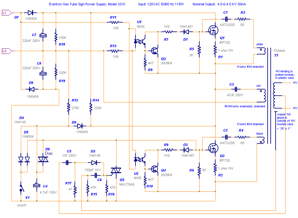
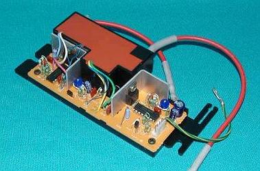
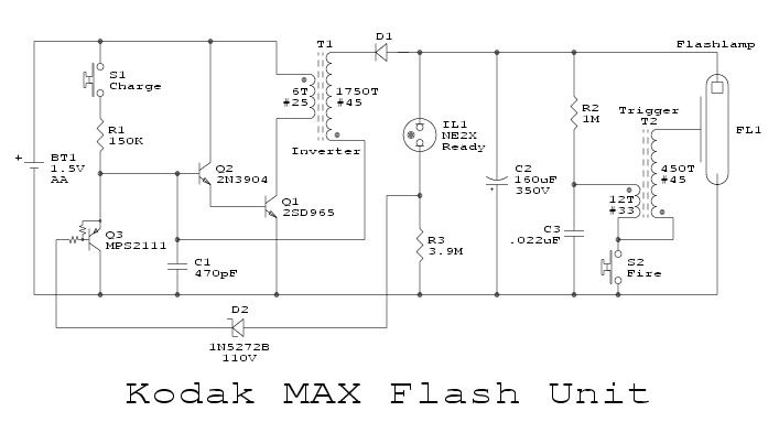
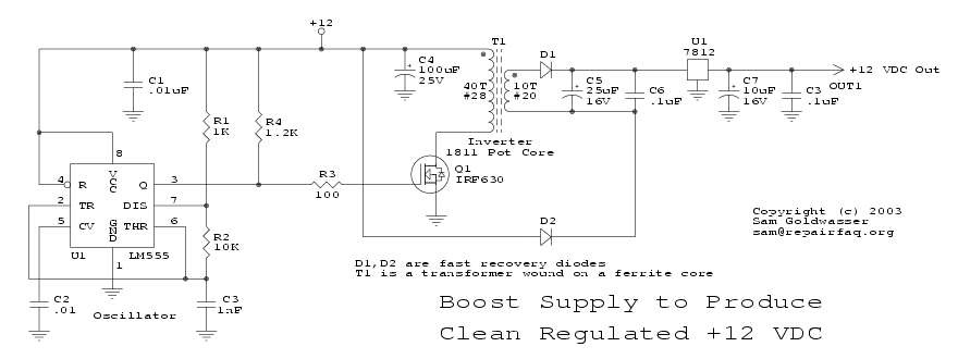
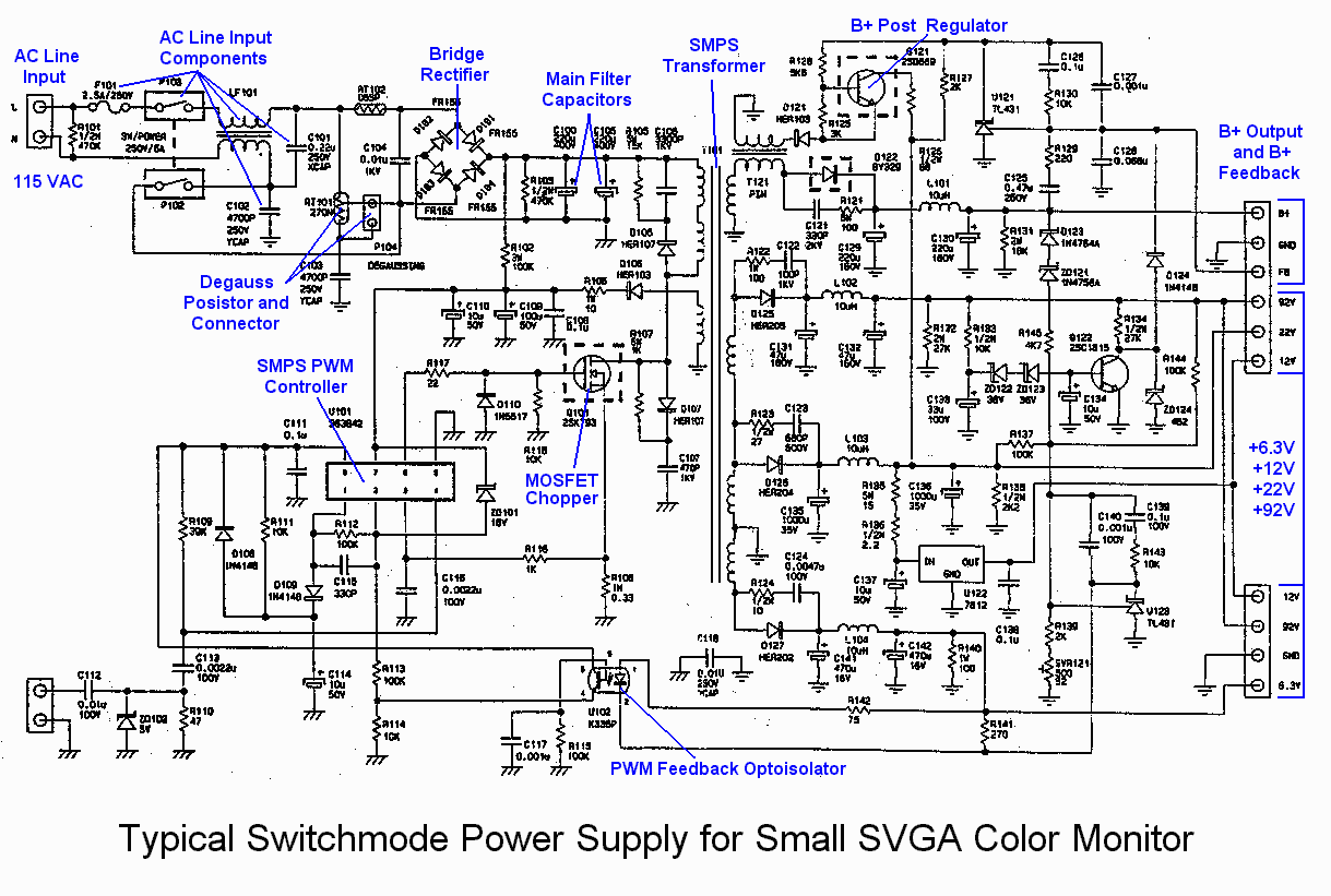
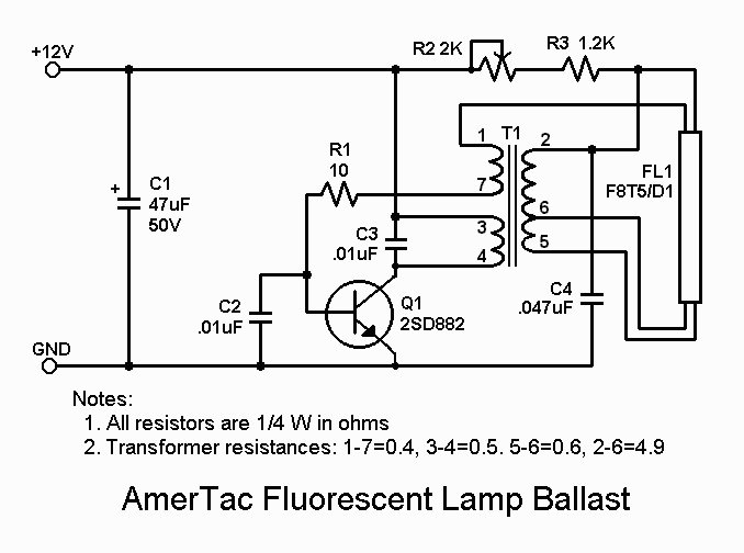
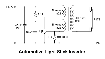
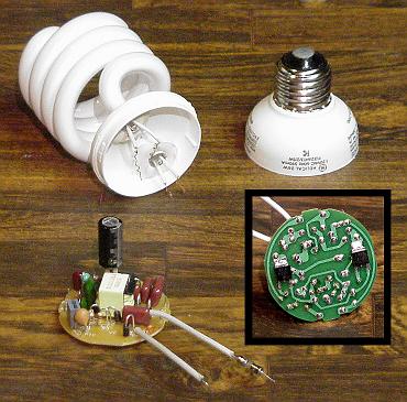
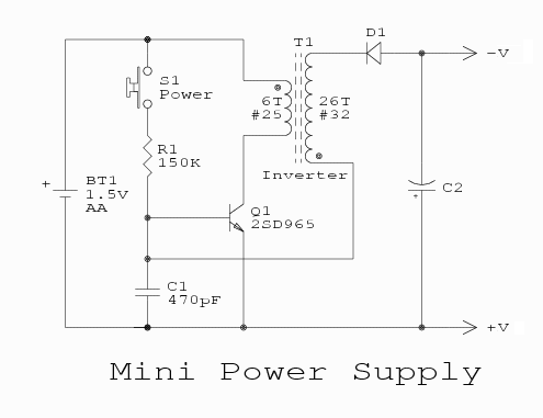
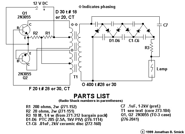
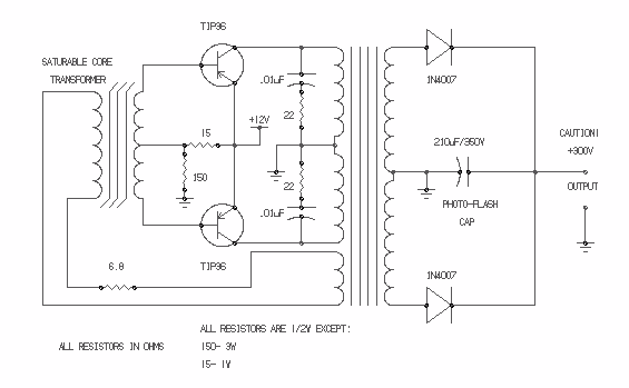
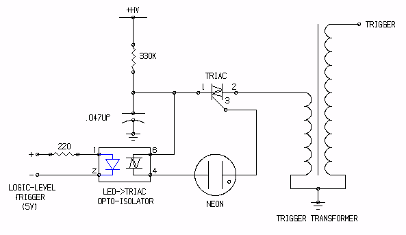
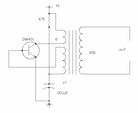
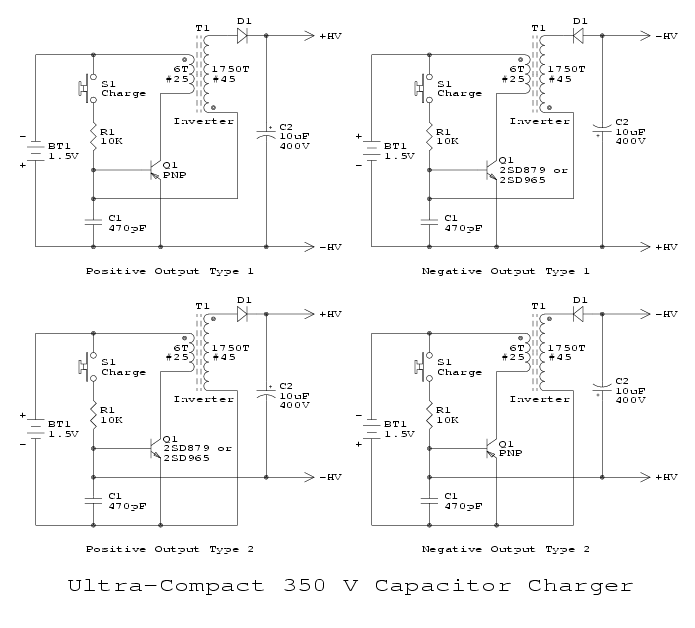
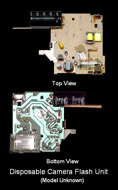
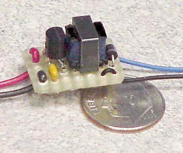
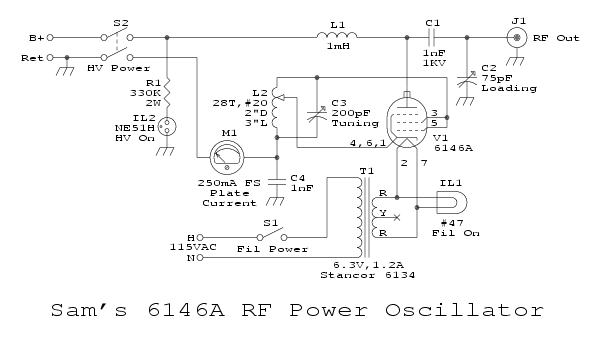
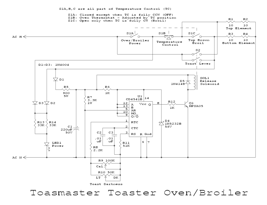
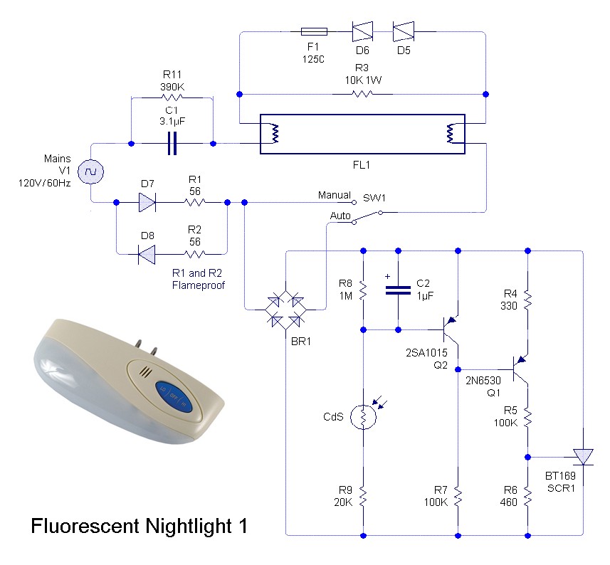
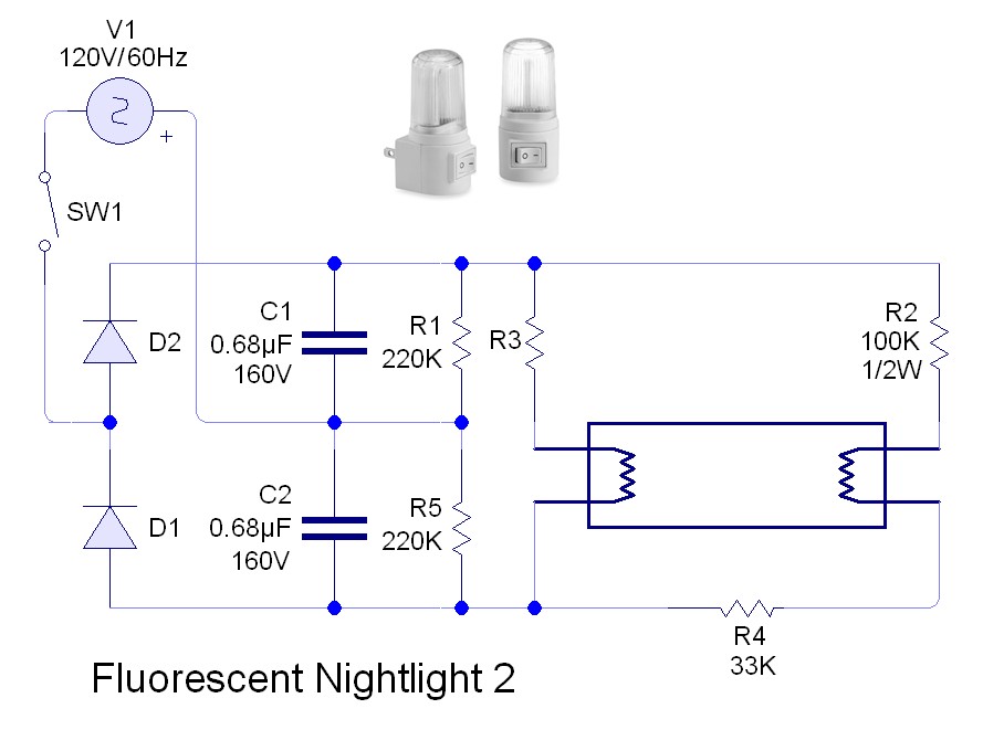
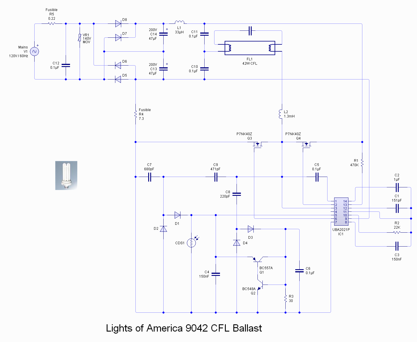
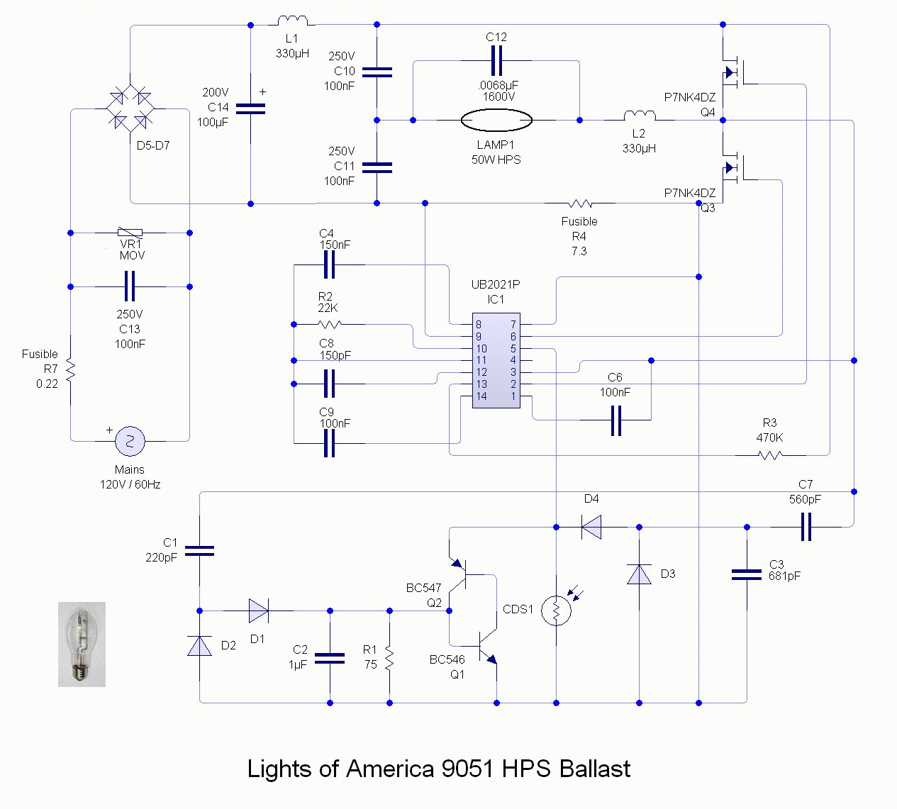
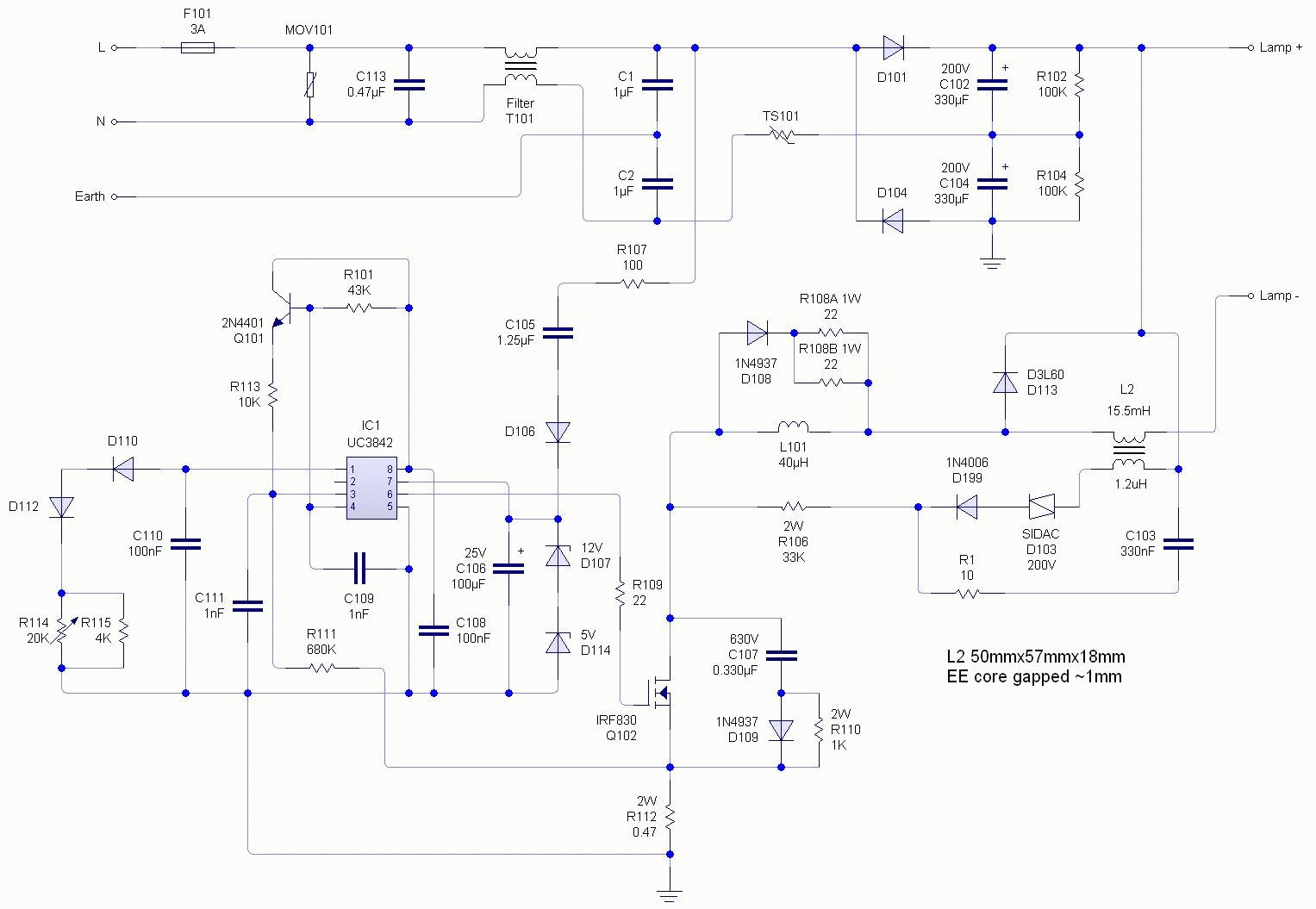
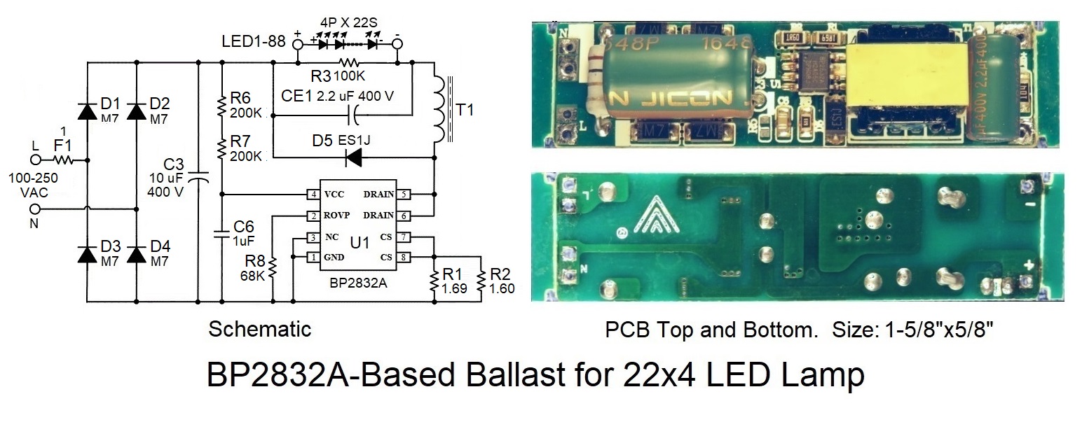