For contact info, please see the Sci.Electronics.Repair FAQ Email Links Page.
Copyright © 1994-2024
Reproduction of this document in whole or in part is permitted if both of the
following conditions are satisfied:
1. This notice is included in its entirety at the beginning.
All Rights Reserved
2. There is no charge except to cover the costs of copying.
DISCLAIMER
µSLC1 is intended for use in hobbyist, experimental, research, and other
applications where a bug in the hardware, firmware, or software, will not
have a significant impact on the future of the Universe or anything else.
While every effort has been made to avoid this possibility, µSLC1 is an
on-going development effort. We will not be responsible for any consequences
of such bugs including but not limited to damage to the wafer FAB you
picked up on eBay for $1.98 + shipping, financial loss from the waste of
28 spools of ABS due to the office 3-D printer fabricating a part with
random dimensions due to loss of lock, or bruising to your pet's ego
from any number of causes directly or indirectly related to µSLC1. ;-)
Acknowledgement
Thanks to Jan Beck for getting me interested
in microcomputer development. If anyone had told me
six months ago that I'd be writing code for an Arduino-compatible
board - and enjoying it (sort of) - I would have suggested
they were certifiably nuts. ;-)
Links to his Web information may be found under
References.
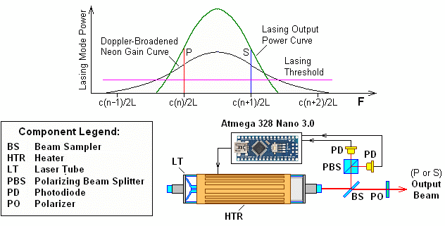
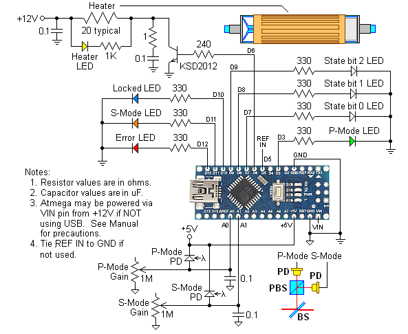
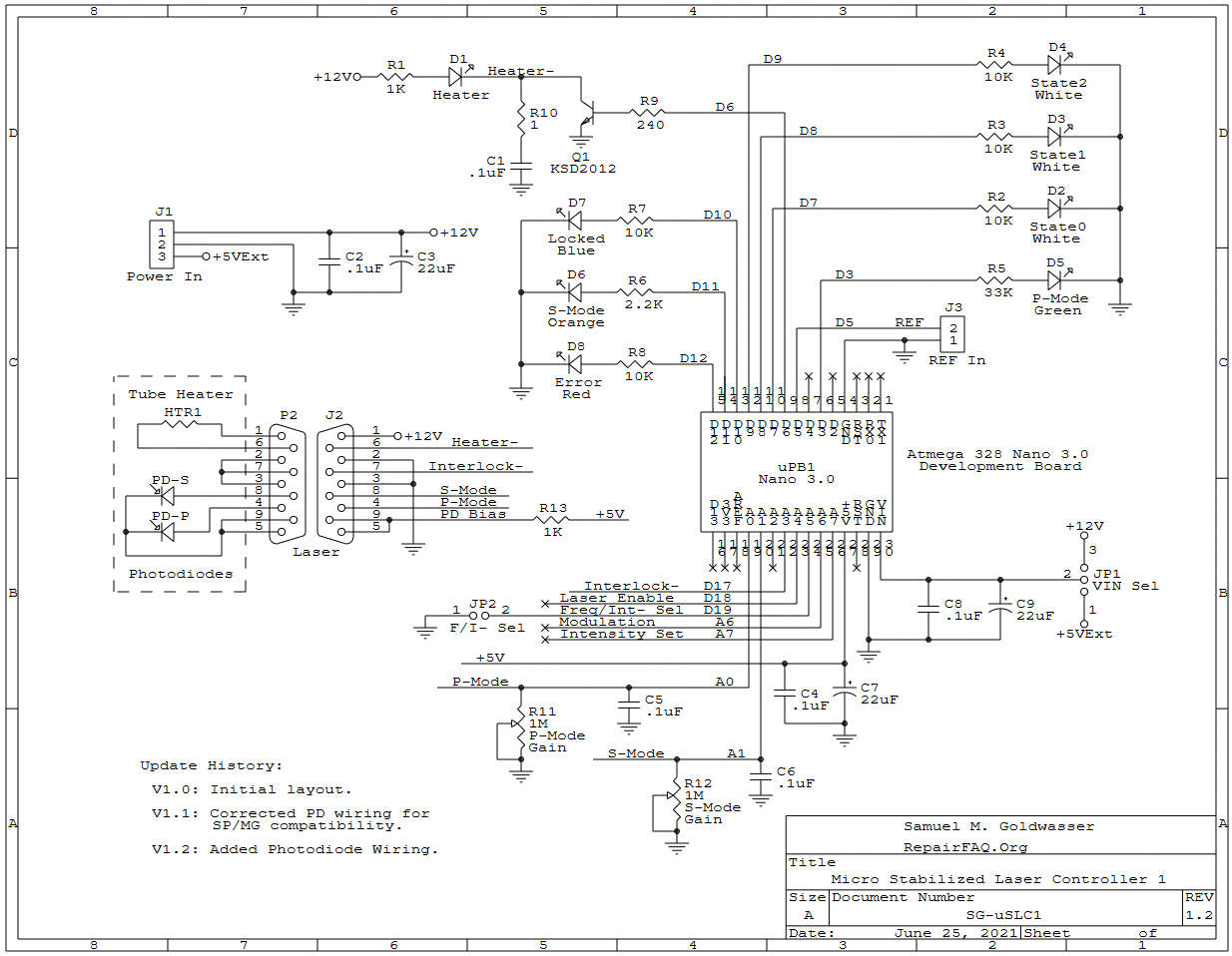
µSLC1 replaces most of the electronic components like op-amps and filter/feedback networks that an analog controller would require with a programmable microprocessor. µSLC1 is not unique in this regard as all but the simplest modern lasers are designed in a similar way. A digital controller is not fundamentally superior to an analog one. However, being easily programmable, it does provide much more flexibility to implement features and optimize performance. µSLC1 is based on a readily available Arduino-compatible Atmega 328 Nano 3.0 board, along with a hand-full of discrete electronic parts. The firmware it runs should be capable of locking virtually any one or two mode HeNe laser (including Zeeman HeNe lasers) which meets certain criteria in terms of size and mode behavior. But if needed, the firmware source code is available and can be easily modified.
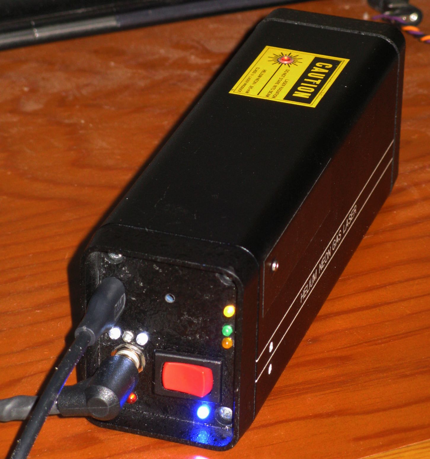
µSLC1 may be used to construct a very compact self-contained laser. The photo below is of a JDSU Novette case - which in itself is among the smallest common (unstabilized) HeNe lasers with a Melles Griot barcode scanner tube and power supply, along with µSLC1 mounted inside including all its LEDs and USB connector on the back-panel. Power is 5 VDC at 2 A provided by a wall adapter. Minor changes to the firmware locking parameters were required due to the low heater power and unvented case. It is a tight squeeze - constructing ships in bottles is probably less stressful. :)
This document provides assembly, installation, and operating instructions for the µSLC1 hardware and firmware to be used with either a commercial laser head like a Spectra-Physics 117A/B/C or a home-built stabilized HeNe laser using, for example, a barcode scanner HeNe laser tube. It also includes µSLC1 Windows Graphical User Interface as an option to enable monitoring of the laser or to control or fine tune locking parameters.
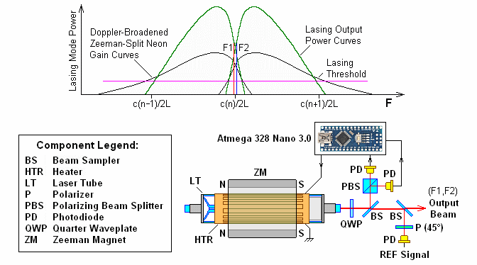
For use with an two frequency axial Zeeman HeNe laser, there are minor changes:
It is assumed the reader is familiar stabilized HeNe lasers and has a need for one. If not, there is probably little reason to be using µSLC1. The output of a stabilized HeNe laser doesn't look any different than that of a non-stabilized HeNe laser (or $1 laser pointer, for that matter). ;-)
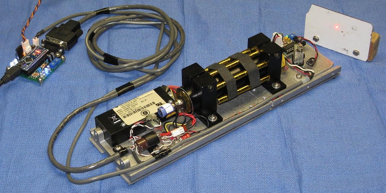
The photo below shows an Axial Zeeman laser built almost totally from scratch. It doesn't even incorporate any HP/Agilent parts except for the recycled 5501A baseplate, but that doesn't count. :) The feedback for stabilization utlizes the waste beam from the back of the tube rather than the front (shown in the diagrams, above). But the REF signal IS obtained via a beam-splitter in the main beam.
The same setup could be configured as a (non-Zeeman) single or dual mode stabilized HeNe laser by removing the stacks of magnets surrounding the tube cylinder and Quarter WavePlates (QWPs) mounted in the blue sleeves at the rear and front (not visible), and adding a polarizer to select the desired mode. Or as a transverse Zeeman laser by doing that and replacing the magnets with ones suitable for providing a transverse field.
With minor changes, µSLC1 could be used with HeNe lasers that have a PZT (PieZo Transducer) for cavity length control like the HP-5501A. It should also be possible to control dual-cavity length systems using a heater around the tube for slow changes and a heater or induction coil on one or both mirror mount stems for fast changes. Other types of lasers (including non-HeNes), as well as devices like tunable filters (etalons), mode lockers, and laser stabilizers might also be adapted to µSLC1. See the section: Variations on µSLC1.
Note: Links to Web pages external to this document will open in a single separate tab or window depending on your browser's settings.
A real-time frequency display for use with axial and transvese Zeeman HeNe lasers is forthcoming. (Locking is unchanged and will work with these lasers now.)
Here is a partial list of suitable commercial laser tubes/heads:
The ATtiny85 version has only a single multi-function LED for status.
Specifications are subject to change without notice. :-)
For a bare tube, ballast resistor(s) and appropriate wiring will also be required. Laser heads may plug into the power supply directly, though adapters or some splicing may be required depending on the plug/sockets on each.
The following are the components required to put together a basic system for the controller. These parts are available from electronics distributors like Digikey and should total no more than around $10 to $15. The Atmega is available from many eBay sellers for as little as $2 delivered. This list does NOT include the laser and its associated optical and electronic parts.
The µSLC1 kits I provide will have most of the following:
µSLC1 should run with at most minor modifications on other Arduino-compatible boards. I did attempt to get the GUI to run on the Pro Micro Atmega32U4, which is even smaller than the Nano. So, it really should be called Pico. ;-) But several issues stood in the way and that project has been shelved for now. The µSLC1 controller (only, no GUI) does run on the femto-size ATtiny85. :)
Designing your own PCB for the bare Atmega IC is also an option but at these prices, it's hardly worth the effort unless the intention is to include it as part of a larger system. This is actually being done for a commercial application. ;-)
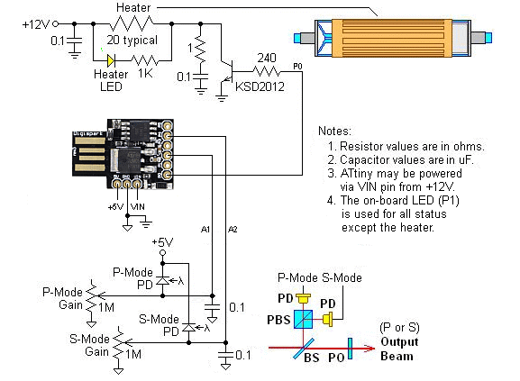
A snubber circuit consisting of a 0.1 uF capacitor and 1 ohm resistor may be required to suppress a turn-off spike due to stray inductance. Aside from unsightly blemishes in the heater drive waveform, the absense of a snubber was resulting in peculiar behavior of the PWM drive and mode input signals.
Note that most of these resistor values have changed compared to those in the previous version of the kits. This is partly due to the annoying extreme brightness of those LEDs using the original resistor values.
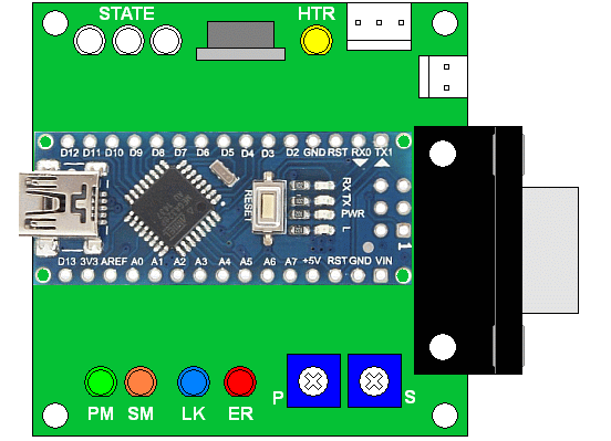
Here is the detailed parts list. The numbering refers to the µSLC1 Schematic and PCB described in the section: Schematic and Printed Circuit Board.
 Prt#  Description                Comments
--------------------------------------------------------------------------------
 uPB1  Atmega 328 NANO             Arduino board with pins soldered

  -    USB A to Mini USB B cable   1 to 3 foot to connect to PC

  -    PCB, µSLC1 V1.1             Updated V1.1 fixes State LEDs,

  -    Socket or strips, 30 pin    For Atmega 328 NANO, recommended for use
                                    with PCB.  May need trimming.

  D1  LED, yellow                  Heater
  D2  LED, white                   State 0
  D3  LED, white                   State 1
  D4  LED, white                   State 2
  D5  LED, green                   P-Mode
  D6  LED, orange                  S-Mode
  D7  LED, blue                    Locked
  D8  LED, red                     Error

  R1  Resistor, 1K ohm, 1/4 W      For Heater LED
  R2  Resistor, 10K ohm, 1/4 W     For State0 LED
  R3  Resistor, 10K ohm, 1/4 W     For State1 LED
  R4  Resistor, 10K ohm, 1/4 W     For State2 LED
  R5  Resistor, 33K ohm, 1/4 W     For P-Mode LED
  R6  Resistor, 2.2K ohm, 1/4 W    For S-Mode LED
  R7  Resistor, 10K ohm, 1/4 W     For Locked LED
  R8  Resistor, 2.2K ohm, 1/4 W    For Error LED

  Note: R1-R8 values are typical and do NOT agree with the schematics.  The
  actual resistors may differ slightly but should be matched to the LEDs
  included in the kit.  Adjust values to balance brightnesses of LEDs if
  these don't result in an adquately pleasing experience. ;-)  The values
  have changed from the past so if you are just getting around to building
  a kit acquired a year ago, some of the old ones may be lower.
  And, no, the 33K for R5 is not a typo.  That value would
  be for a high brightness green LED.  It will be 2.2K for
  a normal green LED - so check it specifically before soldering.

  Or leave off the LEDs and their resistors entirely as the same information
  is available in the µSLC1 GUI. ;-)

  R9  Resistor, 240 ohm, 1/4 W     Heater transistor base drive
 R10  Resistor, 1 ohm, 1/4 W       Heater snubber

 R11  Trim-pot, 1M ohm             P-Mode PD sensitivity adjust
 R12  Trim-pot, 1M ohm             S-Mode PD sensitivity adjust

 R13  Resistor, 1K ohm, 1/4 W      PD current limiting

  Q1  Transistor, power            Heater driver KSD2012 or KSD880 typical

  C1  Capacitor, 0.1 uF            Heater snubber

  C2  Capacitor, 0.1 uF            +12V bypass

  C3  Capacitor, 22 uF             +12V bypass

  C4  Capacitor, 0.1 uF            +5V bypass
  C7  Capacitor, 22 uF             +5V bypass

  C8  Capacitor, 0.1 uF            Vin bypass
  C9  Capacitor, 22 uF             Vin bypass

  C5  Capacitor, 0.1 uF            P-Mode PD filter
  C6  Capacitor, 0.1 uF            S-Mode PD filter

  J1  Screw terminal block or      Power IN
       header, 3 pin.
                                   If header, a mating 3 pin shell and
                                    3 socket pins will be included.

  J2  Connector, 9 pin female RA   Laser head connector
  P2  Connector, 9 pin male        Mates with above
  H1  Hood for above               For laser head cable

  J3  Screw terminal block or      REF IN
       header, 2 pin.
                                   If header, a mating 2 pin shell and
                                    2 socket pins will be included.

 JP1  3 pin jumper block+jumper    Nano power select.

      When using USB power, JP1 can be open.  See CAUTION below if using
      12 VDC power.

 JP2  2 pin jumper block+jumper    Frequency/Intensity mode select

      JP2 can be open - Intensity stabilization is not fully implemented.
      But adding it to the firmware would not be difficult . ;-)
For those not familiar with the common resistor color code (Black/0, Blown/1, Red/2, Orange/3, Yellow/4, Green/5, Blue/6, Violet/7, Gray/8, White/9), the resistors shown above are 150 ohms (brown-green-brown or 15 with 1 zero) ohms and 330 ohms (33 with 1 zero) ohms. The gold stripe indicates 5 percent tolerance on the value but for the use here, tolerance doesn't matter. (It's possible the resistors you use will have 4 stripes where 3 of them are the value and the 4th is the multiplier, along with one for tolerance. If in doubt confirm the value with a multimeter.) The chart below is from Digikey. (If the link decays, a Web search will readily find another one.)

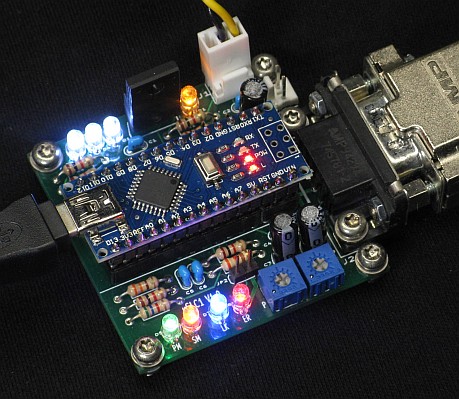
The photo below shows the first version of µSLC1. It matches the schematic/wiring diagram above except for some minor details like specific part values, lack of filter capacitors and snubber, resistors instead of trim-pots for mode gain, and differences in LED colors.
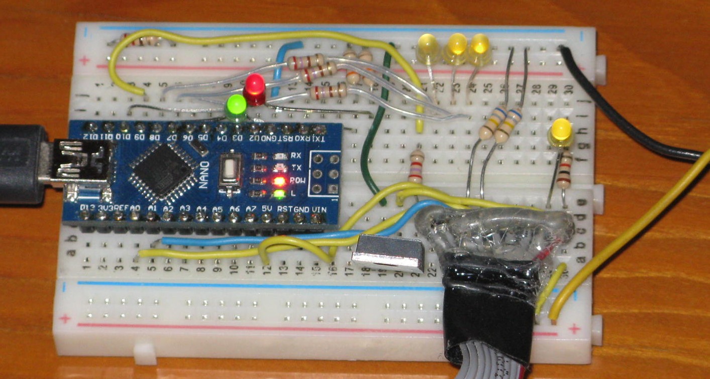
Other parts like jumper wire (solid insulated #22-#26AWG for breadboard connections), cables to attach the PDs and heater, and connectors (if desired) will be required to complete the system.
Most of the connections on the breadboard are made with the electronic parts themselves or bits of excess wire cut from their leads. But there will be a need for a few insulated jumpers which should use #22-#24 solid hookup wire stripped to fit in the holes.
It may be desirable to wire the laser with the photodiodes and heater as a separate assembly, using some sort of connector to attach it to the controller. One suggestion is to use DB9F (controller) and DB9M (laser) connectors wired according to the Spectra-Physics 117/A pinout:
       Pin   Function
     ----------------------
        1    Heater
        2    Interlock
        3    Ground
        4    PD-P Anode
        5    PD-P Cathode
        6    Heater Power
        7    Interlock
        8    PD-S Anode
        9    PD-S Cathode
DC power supplies for the heater (12 VDC at 1 A max assuming a heater of not less than 12 ohms cold resistance) and the Nano 3.0 (5 VDC at less than 1/2 A, unless always connected to USB) will also be required.
CAUTION: The Nano 3.0 can take +12 VDC on VIN since it has an on-board 5 V regulator. But there can be problems when connecting to USB as I found out. Inadvertent ground loops (or something) can result in erasing its brain or damaging the USB chip. Exactly why this occurred is still not clear. The NANO was connected to USB and then the 12 V adapter was plugged in, at which point the USB dropped out, never to be heard from again with this board. The regulated wall adapter was on the same circuit and isolated in any case, so it should not have caused problems. The Atmega microprocessor is still running something so it's not totally dead, thus the suspicion that the problem is the USB chip. But I've been unable to change it so far, even with a programmer. Until the cause can be determined and remedied, it is recommended that USB (or a USB wall adapter) be used to power everything but the heater, which must have its own separate supply even if it runs on 5 V. When used without USB, VIN can be connected to the heater supply if is between 7 and 12 V. Above 12 V, the power dissipation in the LM78M05 on the NANO board could become problematic depending on the current consumption of the LEDs and any other loads. However, an appropriate number of diodes like 1N4004s could be put in series with the heater voltage to drop it to a lower value for VIN. A silicon diode will have a voltage drop of approximately 0.7 V. To summarize: DO NOT attempt to power the Nano board from both USB and either VIN or 5V at the same time.
A few are listed below:
    Manufacturer/Model
  --------------------------------------
    Coherent/Tropel 100,200
    Lasangle RB-1
    Melles Griot 05-STP-901
    Newport NL-1
    REO 32734,33099,39727
    Spectra-Physics 117,117A,117B,117C
    Zygo Axiom 2/20 and 7701,7702,7705
See the info on these and other stabilized HeNe lasers, and other related information in Sam's Laser FAQ under References.
Although the existing µSLC1 PCB (see below) won't fit inside the locking adapter a version lacking the LEDs, or using SMT components could be designed that would. The only additional circuitry required would be the RF induction coil driver. This is little more than an RC oscillator based on a logic inverter, a buffer, and power MOSFET. The photodiode output can be treated the same was as in the normal stabilized laser implementation.
Alternatively (or for initial testing) rather than replacing the original circuitry entirely, it would be possible to tap into the existing locking adapter circuitry to control the RF driver and access the photodiode signal. The driver can be enabled by the normal PWM output from &micr;SLC1 while the normal single photodiode signal is available on a test-point and has a range including 0 to 5 V (though some protection should be added to prevent it from going above 5 V at the microprocessor input). Specifics will depend on which version of the controller is being hacked but it should be straightforward even for the most modern SMT PCB. See the Laser FAQ sections starting with: Aerotech Stabilized HeNe Lasers
Although the standard 05-STP-91x lasers are intensity stabilized, a second photodiode can be easily added for true frequency stabilization, only requiring a hole to be drilled in a cover plate so that the diverted beam from the existing PBS can hit it. (The SMT PCB actually already has hooks in place for frequency stabilization by moving a jumper though this was never marketed. However, the signal on the test-point is probably the offset difference of the two PD outputs so it still may be better to replace the original locking adapter PCB entirely.)
The standard µSLC1 firmware would probably work with minor changes to the locking parameters, but to fully exploit the benefits of the induction heater and also lock near the peak of the output power during mode sweep will probably require some modifications to the code. This is currently left as an exercise for the student but I would be happy to provide technical support via email. ;-)
With some clever modifications, locking on either side of the neon gain curve would be possible. In addition, knowing the shape of the lasing output power curve, it should also be possible to "dial in" a specific optical frequency over a wide range, at least for the 05-STP-912 where it has a more gradual change in amplitude versus optical frequency offset as shown in Comparison of Output Power Profiles of the Tubes used in the Melles Griot 05-STP-910 and 05-STP-912 Stabilized HeNe Lasers. For these lasers, the lasing center wavelength is close to 632.991 nm corresponding to an optical frequency of 473.612 THz. For the 05-STP-912 using the LHR706 tube, the range would be +/-600 MHz except for a small area at exact line center and possibly up to 200 MHz on the blue side which is nearly flat and so could be tricky. (Beyond around 600 MHz on either side, a second mode may pop up.) The lasing output power curve of the LHR704 tube in the 05-STP-910 (as shown in the above graphic) is relatively flat within around 350 MHz of line center, so locking there would probably not be possible.
These tasks are also left as an exercise for the student. :)
PCB Version 1.1 is now available. It has corrected the
layout errors of V1.0. If you have a V1.0 PCB, see
µSLC1 PCB Version 1.0
Corrections.
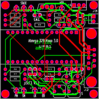
The Nano 3.0 board should installed in a socket so that in the unfortunate circumstance that is goes bad (these things can happen!), replacement is straightforward. Attempting to desolder the Nano from the µSLC1 PCB without damage would be difficult. It will not fit in a machined pin socket but will in a leaf spring socket. However, 30 pin sockets are difficult to find so making one up out of pieces of a pair of 24 pins sockets, a 40 pin socket, or two 15 pin strips may be required. A 40 pin leaf spring socket or pair of 15 pin strips is included in the kit.
Since the brightness versus power for LEDs can vary dramatically depending on type and color, the current limiting resistors for the LEDs should be selected before soldering to equalize their brightness (if you care). For the LEDs I used, this required the resistance to range from 330 ohms to 33K ohms. That is not a type - the blue, green, and white LEDs are much more sensitive than the others.
The 3 pin header is for power (+5 Ext, GND, +12V). The +5V Ext is optional for VIN rather than 12V. The 2 pin header is for the REF frequency input for use with Zeeman lasers. Screw terminal blocks may be substituted for the headers and make assembly and connections simpler, but don't allow the PCB to be unplugged easily.
The remainder of the board is taken up with mundane things like resistors and capacitors. ;-) Since its size is mostly limited by the Nano and DB9F, using SMT components would not be very beneficial and would make hobbyist assembly and modifications (and mine!) more of a pain.
Regardless of whether you decide to use the PCB, it may be desirable for the system to be first built up on a solderless breadboard to confirm that the default components are satisfactory. Depending on the specific laser tube, the waste beam (of sampled beam) may be lower or higher in power than what is optimal for the P-Mode and S-Mode adjustments. The snubber RC network may also need to be modified depending on the laser head cable length and type. Also, LED brightness can vary significantly and their current limiting resistor values may need to be changed (probably to higher values to reduce the brightness). With my assortment of LEDs, the resistor ranged from 330 ohms to 5.6K ohms to match brightness. Of course, there's no need to install all the LEDs but they do add a touch of class. :) If 330 ohm resistors are used for the State LEDs, the thing can probably be used as a reading light in Error State 7. :( :)
 Arduino Pin   Physical Pin   Function
--------------------------------------------------------------------------
     D3             6         P-Mode LED (5V PWM, 0 to 100 percent)
     D5             8         REF Frequency input (TTL 0 to ~6 MHz)
     D6             9         Heater Drive (5V PWM, 0 to 100 percent)
     D7            10         State bit 0 LED (0 or 5V)
     D8            11         State bit 1 LED (0 or 5V)
     D9            12         State bit 2 LED (0 or 5V)
    D10            13         Locked LED (0 or 5V)
    D11            14         S-Mode LED (5V PWM, 0 to 100 percent)
    D12            15         Error LED (0 or 5V)
    D13            16         Heartbeat LED (Atmega "L")

     A0            20         P-Mode input (0 to 5V)
     A1            21         S-Mode input (0 to 5V)
     A2            22         External Modulation input (future, 0 to 5V)

    +5V            27         +5 VDC from on-board regulator or USB
    VIN            30         Optional DC input (+7 to +20 VDC)
    GND           4,29        Ground/Common
See CAUTION above with respect to power.
To compile and upload the firmware (either initially or to make any changes) and to run the Windows GUI will require a Window PC or laptop. Almost any vintage machine should suffice as long as it has at least one USB port and Microsoft Net Framework 4.0 or later is or can be installed. The µSLC1 GUI has been tested on Windows XP, 7, and 10. It should run on anything in between, but this has not been confirmed. More on the software support environment below.
There are many ways of doing this - some which may be overly complex, but what I've done for the Atmega 328 Nano 3.0 board is to go to Arduino Software and install the current version of the Arduino IDE (V1.6.9 as of May 2016). (I'm not sure if the board needs to be plugged in to a USB port during this process, but mine was. During the install process, it will ask to install the drivers. Reply "Yes" to all its requests. When the Arduino IDE is started for the first time, go to "Tools", "Board", and select "Arduino Nano". If the Nano is plugged in, its COM port should appear under "Tools", "Port". If you received the Nano from me, it will have µSLC1 firmware. Go to "Tools", "Serial Monitor". The Serial Monitor windows should appear and after a few seconds start pumping out data from the board. Select a baud rate of 57600 to turn it into something meaningful. With no laser, the data should look something like:
 0 0 0 9745 8 6104
 0 0 0 9746 10 144
 0 0 0 9747 11 5
 0 0 0 9748 15 260
(The 4th value is a sequence number which should be incrementing by 1.)
More info on software, drivers, and more at Getting Started with Arduino and Genuino on Windows.
The more complex installations may be required if you bought the Nano from eBay or off the back of a truck, depending on whether it has the genuine FTDI USB communications chip. And even more complex if it doesn't have the bootloader installed. Links for driver installation may be found under References under "Arduino". Instructions for burning the bootloader may be found in the section: Burning Bootloaders into the Nano or Pro Micro.
The Arduino IDE can be used for compiling and uploading, though I prefer UECIDE, below, because compilation and uploading is much faster. For use with the Atmega328 Nano 3.0, either is fine. However the ATtiny and Pro Micro may only be supported by the Arduino IDE. (The latter may come up as Arduino Leonardo though.)
The UECIDE files should be unzipped to any convenient location on your computer. UECIDE requires around 160 MB there, and another 600+ MB for support files typically somewhere like c:\users\YourUserID\AppData\Local\UECIDE. This location can be changed in File->Preferences. If doing this after having configured UECIDE, copy all the files to the desired destination first, then change the data directory in File->Preferences. DO NOT delete the original UECIDE directory or the preferences file! :) Otherwise, the configuration information will all be lost.
Compared to most applications, UECIDE takes forever to start up even on a fast PC. So be patient. That's the bad news. The good news is that compiling and uploading takes literally only a few seconds, much faster than with the Arduino IDE or MPIDE (another one you don't need to know about). Go figure. :)
The first thing UECIDE will likely do is to tell you that no boards are installed and then open the Plugin Manager. If it does not, do it manually by going to Tools->Plugin Manager. At first the pane along the left will only show the word "Plugins". But after a couple minutes, it should update with a list: Plugins, Libraries, Boards, Cores, Compilers, System. The following are required:
For each of these click on "Install". Installing the arduino board will probably automagically install the other related files and may take several minutes. Confirm that each entry has a green check mark next to it.
Close the Plugin Manager and go to "Hardware" or check the status line at the bottom of the window to confirm that the proper Board (Arduino Nano w/ Atmega 328), core (Arduino 1.6.x)), and Compiler (GCC 4.8.1 for AVR) has been selected. Correct it if not.
Some other quirks of UECIDE that I've found:
Plug the Atmega board into any available USB port. The power LED should come on. If I (Sam) sent you the Atmega board, it will have been loaded with a version of the µSLC1 firmware and the user LED will be flashing at about a 5 Hz rate to let you know it is alive. Run the µSLC1 GUI and check the firmware revision (Help->About). If it doesn't match the one above, it may be a good idea to update it.
Assuming the driver has already been installed, go to Hardware->Serial Terminal and select its COM port. Typically, this will be the highest number COM port, or perhaps the only one, since no one uses real COM ports for much of anything anymore.
UECIDE should remember the configuration settings automatically upon exiting. These are tied to each instance of the UECIDE window, so it's possible to easily deal with multiple totally different board types.
   Compiling...
     * Compiling sketch...
     * Compiling core...
       > arduino
     * Compiling libraries...
     * Linking sketch...
   Compiling done.
   Memory usage
     * Program size: 7532 bytes
     * Memory size: 1092 bytes
     * Compilation took 8.634 seconds
   Uploading firmware...
     * Resetting board...
     * Uploading...
     * Resetting board...
     * Upload Complete
Once the firmware has started, all the LEDs will come on at full brightness for 2 seconds as a sort of "Lamp Test" (including the Heater LED if the heater supply is on) and then the on-board LED "L" should be flashing at a 5 Hz rate to let you know it's alive.
The firmware is retained in non-volatile memory so uploading only needs to be done once - or until a new version is available!
Uploading new firmware does not affect the user locking parameters stored in Atmega EEPROM. However, should the format change (rarely), the firmware will revert to the default locking parameters. In that case user parameters that differ from the defaults will need to be re-entered via the GUI Command window and then saved.
The firmware may also be compiled without uploading by using Ctrl-R. Since you haven't messed with the code, it should compile without errors. This is slightly faster for testing and doesn't use the board at all so it can be off doing whatever it pleases. :)
The latest µSLC1 GUI may be downloaded from uSLC1_GUI.1.0.6284.18461.exe.
Save the µSLC1 GUI .exe file into any convenient directory. (There's a small chance that the first time it's run, an error is produced since there is no configuration file associated with it. Simply continue and the GUI will come up. When it is closed using "Finish", valid settings will be saved so that the error should not appear again.)
Important: DO NOT reset the board while the µSLC1 GUI is running. The GUI will need to be aborted, the board may need to be reset again, and only then can the GUI be restarted. However, the GUI may be aborted and restarted ad-infinitum without affecting the firmware and laser. ;-) (However, installing or removing the USB cable may reset the firmware.)
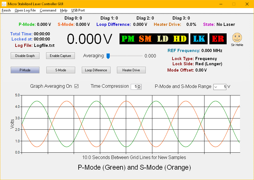
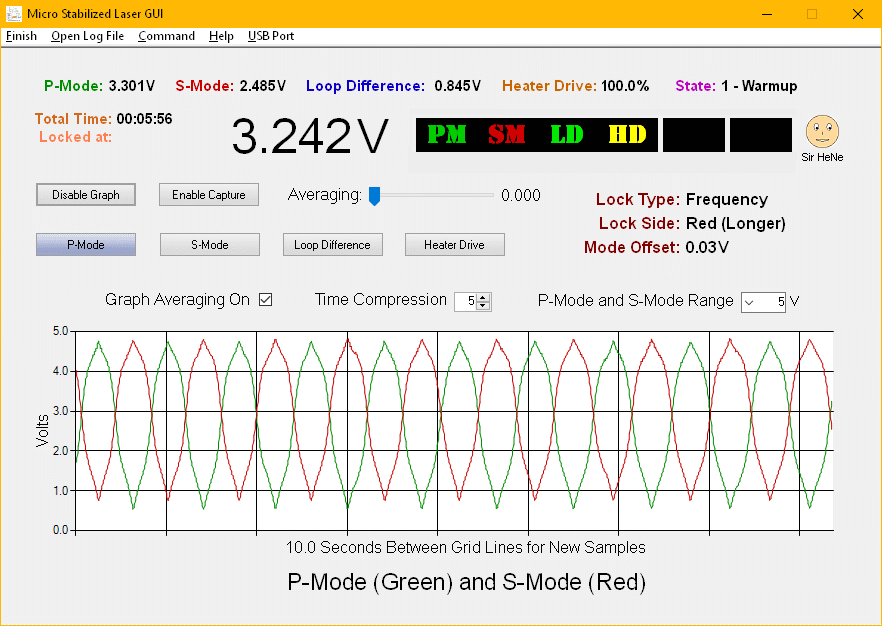
The graphic below shows the typical GUI main window at startup.
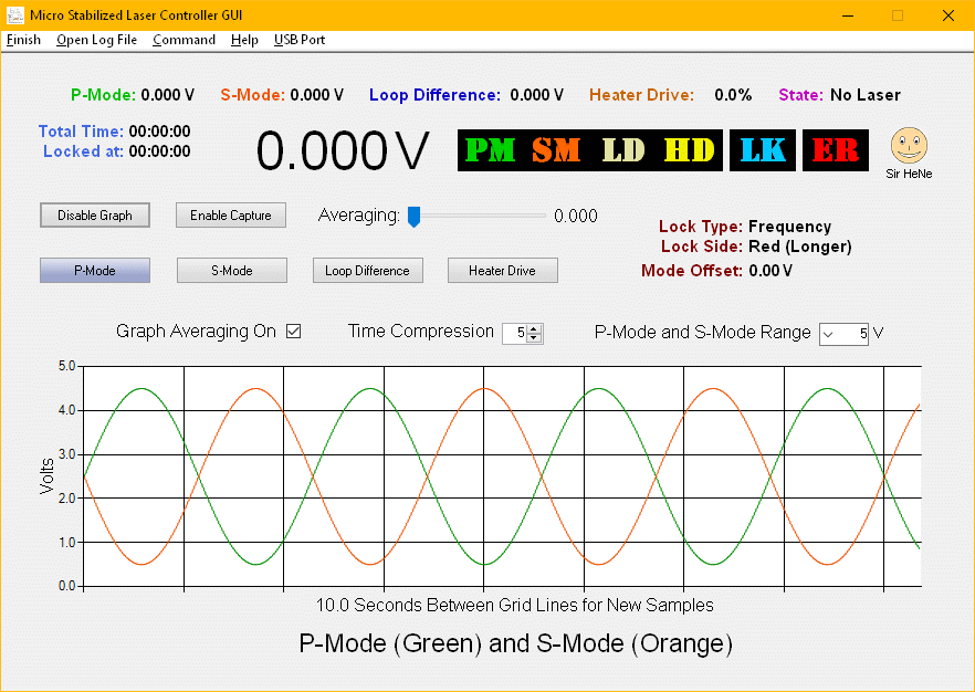
Yes, this bears remarkable similarity to the µMD1 GUI due to having inhereted much of its DNA. ;-) When first started, all the readouts are loaded with zeros and the fake LEDs are turned on to show that they are there. Sort of a high tech "lamp test". ;-)
Important: The GUI can be started at any time but the firmware must be running before the USB COM port is selected or else the Universe may implode or explode, which one occurs and when has yet to be determined. :) Confirmation of this issue is left as an exercise for the user. ;-) There should be no need to reset the firmware when restarting the GUI - it will pick up where it left off.
Note that the GUI is NOT required to run the laser with the µSLC1 controller and starting or restarting the GUI has absolutely no effect on laser behavior. (Or at least it shouldn't.) Unless messing with the parameters in the "Laser Firmware Hacking" (Command) window (which will be explained below), for most users, the GUI will only be used to monitor the laser. Actually, for most laser users, there is no need for the GUI at all! It's there primarily as a development aid and for unapologetic laser jock technoduibes. ;-)
The first set are the selection buttons at the top of the window. Note that except for USB Port, these do not invoke drop-down menus and require only a single click to activate.
The log file is closed and its name and path are saved upon exiting the GUI.
These buttons may all be accessed via Alt-first letter.
The next set are the buttons for selecting what's shown in the Main Readout and what is plotted:
The log file format is: PM:P-Mode SM:S-Mode HD:Heater Drive SN:Sequence Number LSC:Low Speed Code LSD:Low Speed Data.
      Item       Abbrev    Data Range    Value/Range
 -------------------------------------------------------
     P-Mode        PM       0 to 1023     0 to +5 V
     S-Mode        SM       0 to 1023     0 to +5 V
  Heater Drive     HD        0 to 255   0.0 to 100.0 %
  Sequence Number  SN        0 up :-)   Time * 977 / 16
  Low Speed Code   LSC      16 bit int       --
  Low Speed Data   LSD      32 bit int       --
Low Speed Code and Low Speed Data are used to return information that doesn't need to be displayed at the sample rate like State, Lock Time, and firmware version, and read back the locking parameters from the firmware, and monitor other aspects of the firmware.
A typical snapshot of a logfile is shown below:
   Sample Frequency = 61.04 Hz

   PM:594 SM:601 HD:142 SN:9743 LSC:0 LSD:0
   PM:596 SM:604 HD:142 SN:9744 LSC:12 LSD:1590
   PM:599 SM:606 HD:142 SN:9745 LSC:8 LSD:6104
   PM:598 SM:604 HD:143 SN:9746 LSC:10 LSD:144
   PM:594 SM:600 HD:143 SN:9747 LSC:11 LSD:5
   PM:596 SM:604 HD:142 SN:9748 LSC:15 LSD:260
   PM:600 SM:604 HD:143 SN:9749 LSC:0 LSD:0
   PM:599 SM:604 HD:143 SN:9750 LSC:0 LSD:0
   PM:599 SM:605 HD:143 SN:9751 LSC:0 LSD:0
   PM:599 SM:606 HD:142 SN:9752 LSC:0 LSD:0
   PM:596 SM:601 HD:143 SN:9753 LSC:101 LSD:0
   PM:596 SM:601 HD:143 SN:9754 LSC:102 LSD:0
   PM:597 SM:600 HD:144 SN:9755 LSC:103 LSD:0
   PM:597 SM:601 HD:143 SN:9756 LSC:104 LSD:2
   PM:597 SM:602 HD:143 SN:9757 LSC:105 LSD:1
   PM:596 SM:601 HD:143 SN:9758 LSC:20 LSD:0
   PM:598 SM:603 HD:143 SN:9759 LSC:0 LSD:0
   PM:599 SM:604 HD:143 SN:9760 LSC:12 LSD:1593
   PM:596 SM:600 HD:144 SN:9761 LSC:8 LSD:6104
The Sample Frequency is 1/16th of the firmware control loop update rate derived by: 16 MHz (Atmega I/O Clock) / 64 / 256 = 976.56 Hz. 976.56 Hz / 16 = 61.04 Hz.
The Averaging coeeficient is saved upon exiting the GUI.
The Time Compression factor is saved upon exiting the GUI.
Exit from State 7 to State 0 if no laser light after a long time, or to State 1 if the laser beam reappears. The firmware is persistent though - it will keep trying for a long time. :-) There is no error checking in States 2, 4, or 6.
Before a USB port is selected, State will display "No Laser".
When the firmware is started (power on to the board, reset, or just after the firmware is uploaded), the controller enters State 0, Startup. When it detects laser output, it goes to State 1 which drives the heater at full power while monitoring the length of the mode sweep cycle.
The graphic below shows a snapshot of the Main Window about halfway through warmup. The mode sweep cycle at this point is around 8 seconds.
Once the mode sweep cycle time exceeds the "Mode Period" value, the controller goes to State 3, Locking. There it checks for the Loop Difference to settle down below the "Locking Tolerance" value. It then goes to State 5, Locked.
The graphic below shows a snapshot of the Main Window just after the laser has locked. On the left portion of the graph is the laser mode sweep of the P-Mode and S-Modes prior to locking.
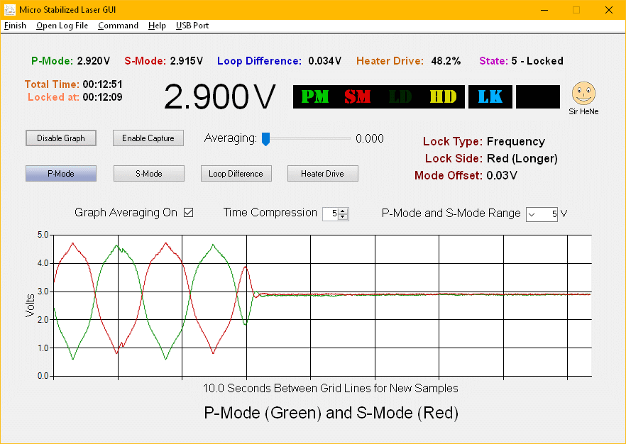
The laser will remain locked forever unless the P-Mode or S-Mode go bonkers (technical term!). If it does go bonkers, the controller will go to State 7, Error and try again.
Data from the Atmega board is sent at a rate of just over 60 pps. At a compression of 5, the time between horizontal divisions is close to 10 seconds. However time compression of the plot may be set up to 1,000 so that more than 2 hours of data may be visible. Although the data is only subsampled, not averaged, graph averaging can do something similar.
The way these affect the firmware operation differ based on whether it is a state change or parameter change:
CAUTION: Messing with many of the following will result in a laser that never stabilizes (at least until the firmware is restarted or reset to default values). However, permanent damage to anything but your ego is unlikely.
State Commands (and their parameters)
State 0 will remain in effect for a minimum of 2 seconds simply to enable it to appear in the State LEDs or GUI. :)
Note that for States 2, 4, and 6, if the heater drive is selected to be other than 0% or 100%, the value displayed in the Heater Drive readout(s) may differ by a fraction of 1 percent from the requested power due to roundoff error in conversion from the range of 0 to 100% that us humans understand to the PWM range of 0 to 255 and back again. Live with it. :)
If none of the state or locking parameters (below) have been changed, restarting (going to State 0 or resetting or reloading the firmware and GUI) will generally restore your laser to supreme happiness (assuming it ever was supremely happy). ;-)
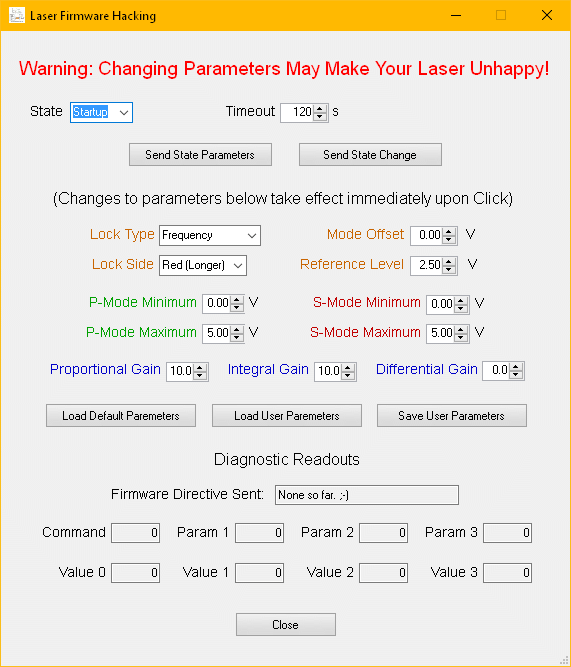
Firmware locking parameters
These take effect as soon as a widget is "clicked" (up or down), but not by simply changing its value.
Load/Save
The parameters that control locking are stored in the Atmega. There are three 32 word data structures:
For reference, the LCB, DCB, and UCB format is as follows:
 Location   Parameter           Range/Value
-------------------------------------------------------------------
     0      EEPROMFormat        Firmware compatibility value
     1      PmodeMin            0 to 818 for 0 to 4 V (0 V)
     2      SmodeMin               "              "   (0 V)
     3      PmodeMax            205 to 1023 for 1 to 5 V (5 V)
     4      SmodeMax               "              "      (5 V)

     5      ModePeriod          10 to 1800 for 1 to 180 s (14 s)

     6      ControlRegister     Lock Side:
                                  Bit 0 = 0: Red
                                  Bit 0 = 1: Blue

                                Lock Type:
                                  Bits 2:1 = 00: Frequency
                                  Bits 2:1 = 01: Intensity P-Mode
                                  Bits 2:1 = 10: Intensity S-Mode

     7      LockingTolerance    1 to 511 (8)
     8      ReLockCount         0 to 9999 (1)

     9      ProportionalGain    0 to 32 (10)
    10      IntegralGain        0 to 32 (10)
    11      DifferentialGain    0 to 32 (0, presently ignored)

    12      Duration0            10 to 6000  for  1 to  600 s (120 V)
    13      Duration1           100 to 18000 for 10 to 1800 s (180 V)
    14      Duration2            10 to 6000  for  1 to  600 s (30 V)
    15      Duration3            10 to 3000  for  1 to  300 s (20 V)
    16      Duration4            10 to 18000 for  1 to 1800 s (15 V)
    17      Duration5           300 to 18000 for 30 to 1800 s (300 V)
    18      Duration6            10 to 18000 for  1 to 1800 s (360 V)
    19      Duration7            10 to 18000 for  1 to 1800 s (120 V)

    20      HeaterValue0        0 to 100 percent (0 %)
    21      HeaterValue1           "        "    (100 %)
    22      HeaterValue2           "        "    (100 %)
    23      HeaterValue3           "        "    (50 %)
    24      HeaterValue4           "        "    (0 %)
    25      HeaterValue5           "        "    (50 %)
    26      HeaterValue6           "        "    (0 %)
    27      HeaterValue7           "        "    (0 %)

    28      Spare1

    29      Offset              0 to 1023 for 0 to 5 V (0 V)
    30      Intensity              "              "    (2.5 V)

    31      CheckSum            Not implemented
Ranges and default values subject to change without notice. ;-)
When the firmware starts, the DCB is copied to the LCB unless a valid UCB has been saved, in which case it is copied to the LCB. The LCB is then read out of the Atmega over USB into the GUI Command Window widgets. When a NANO board is loaded with firmware the first time ONLY, the DCB is copied to the LCD and saved as the UCB.
Note that while there is no way to save the locking parameters to a file explicitly (and there never will be!), a record can be made of them by starting the GUI, opening a log file, enabling capture, and then opening the USB Port. The first thing the GUI does is to upload the LCB in use from the firmware which will show up in the log file as a consecuative 32 sample block near the start with Low Speed Codes from 130 to 161. Reformatting as desired is left as an exercise for the determined student. ;-)
The next set of widgets are for diagnostic purposes. If they don't seem to make any sense, that's by design and it shouldn't keep you up at night. ;-)
The state of this Checkbox is saved when the GUI is terminates.
And finally, the quickest way out of the hacker's window:
However, the Command Window does NOT need to be closed to do things in the Main Window.
If any of the parameters have been modified in the GUI and sent to the firmware but not saved, exiting the GUI (X or Finish) will ask if they should be saved before actually relegating them to the bit bucket. However, as noted, even if not saved, they are still in Atmega memory as long as the board hasn't been reset or power cycled. So, if the GUI is restarted, they will be retrieved automagically and can still be saved via the Command window. :)
Note that any changes made in the Command window before opening the USB Port will be lost when it is opened and the LCB is uploaded automatically from the firmware.
Note: The following assumes the use of the Atmega Nano 3.0 board. If you've somehow figured out how to get the Pro Micro, change any references below to pins as appropriate. If you're using the ATtiny, there is no GUI support, period. So any failure of the GUI to do anything is a feature, not a bug. ;-)
The first set of problems deal with the board independent of the GUI and assumes that all the LEDs are present. However, some also apply to the readouts of the GUI. "LEDs" below refer to either physical LEDs or the fake ones of the GUI, as appropriate. ;-)
If there are problems uploading firmware and/or opening the COM port in the GUI AND your Nano board has the CH340 USB chip (which includes anything I provide), especially if it has no label, it may be incompatible with the CH340 driver currently installed on your system. The typical error when uploading is:
 avrdude: ser_open(): can't set com-state for "\\.\COM3"
 An error occurred while uploading the sketch
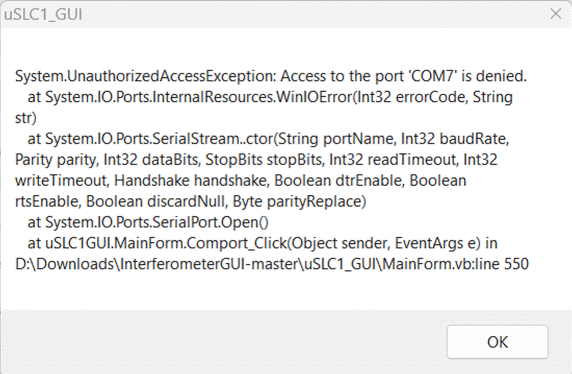
If already loaded, attempting to open a COM port in the µSLC1 GUI, will generate a block of errors similar to uSLC1 Errors when Opening COM Port with New CH340 and 2023 Driver and do nothing useful. So even if you have no interest in modifying the firmware, this issue may still exist.
With the Nano board plugged in, determine what version of the device driver is installed by going to the Windows Control Panel, "Device Manager", "Ports (COM & LPT). Then double click on "USB Serial CH340....". Go to "Driver". If it is a version later than 2019 (probably 2023 or 2024), it may not work depending on the CH340 chip. (I know this issue exists with the 2023 driver but haven't tested a known quirky Nano with the 2024 driver yet.)
DO NOT UNINSTALL THE DRIVER as that may delete it entirely and make it unavailable should there be a need to get it back. Go to "Update Driver", "Browse my computer for drivers", "Let me pick from a list of available drivers". Hopefully an older version is still there. Both the 2014 and 2019 versions are known to work with these Nanos. Else install the 2019 version which may be found under References: CH340 Windows USB Driver Installer (2019)(Local). Even with the older driver, there may still be some flakyness in uploading. Note that a subsequent Windows Update will likely resintall the 2023 driver (or whatever the latest version is). Without doing that, even just using a different USB port may result in the later driver reappearing. More info and fixes at: Arduino Counterfeit Fake CH340G chips driver issues.
Even with the 2019 driver, the upload may hang. Press the Reset button on the Nano and it should then go through the normal upload sequence and terminate without errors. Go figure. :( ;-)
I will attempt to avoid Nanos using these bogus parts, but there may be no choice after a while. It is really too bad that the original Nanos are so expensive - Almost 10X the cost and even available.
Check the polarity of the physical LEDs. The cathode (flat) should point away from the output pin. Confirm the value of the resistors to be 330 ohms, or in the vicinity. The resistors should go to GND. Check the output voltage from the Arduino pins D10 and D11.
The following problems are GUI-related:
More coming soon.
There is also a version of this board labeled "ATtiny85" which should be functionally similar but with a slightly different layout and a proper USB connector. :)
The single on-board LED serves as a multi-mode status display (documented in the firmware). To further simplify the circuit, eliminate the Heater LED, but then it would be boring. :)
VIN goes directly to a 78L05 regulator so the +12 VDC for the heater could be used to power the board when not connected to USB. DO NOT use them both at the same time. CAUTION: There is no protection on +5V power. So when connected to USB, any wiring mistakes or failures that result in excessive current from +5 VDC to GND will pull it from the USB port. Depending on the computer's USB subsystem, this could be bad. It has been suggested that connecting the ATtiny board through a USB port replicator or hub might provide better protection. USB is supposed to handle overloads gracefully but not all implementations do.
Note that there are two versions of this board: 5 V/16 MHz and 3.3 V/8 MHz. There is no point in using the latter unless you have a specific need for lower power (like this matters with a power gobbling HeNe laser!) or to be 3.3 V compatible. Confirm the version before buying.
However, I have more or less given up on going any further with the Pro Micro. There were just too many issues that didn't have obvious solutions. These relate to the Arduino IDE, windows driver, Pro Micro hardware, and probably the firmware. I do not know whether they are independent, or if a single mater issue is at work here.
After (6) occurred, it wasn't clear whether the microprocessor got fried, a USB pin became disconnected on the board, or the bootloader firmware became corrupted. But I figured I would attempt to reload the bootloader just in case based on Burning Bootloader on Pro Micro. The plan was to use an Atmega 328 Nano 3.0 as the Arduino ISP. After wiring it as in the description and plugging it in, both boards appeared to be receiving power but then my PC belched up the "Blue Screen of Death" and rebooted. The error had something to do with closing the USB driver improperly. Exactly how that could have been caused by the wiring between the two boards is not at all clear. I'd never seen any manner of screwup on a USB device crash Windows before.
Not to give up just yet and still hHoping that the problem was a corrupted bootloader, I loaded Arduino 1.6.9 with the Pro Micro add-in and Nano driver on a non-critical XP laptop (just in case bad things happened) and tried again. This time nothing bad happened and the bootloader was burnt sucessfully, so the Pro Micro is back in shape. (See the detailed procedure below adapted specifically for use with the Atmega 328 Nano 3.0 as the ISP.) However, issues (3), (4), and (5) persist. To keep the board preoccupied and happy for now, I loaded an alternating RX/TX LED blinkie sketch. ;-)
If anyone is interested in pursuing the Pro Micro-based µSLC1, the firmware may be downloaded at µSLC1 Pro Micro Firmware Version 03. It compiles, but has not been tested with a laser and it may have coding bugs not related to anything else even though most everything was copied from the Nano version. Change the pin locations in the Atmega 328 Nano 3.0 wiring/schematic based on the comments in the firmware. However, given that the primary advantage of the Pro Micro is a very slightly smaller form-factor, the hassle of working through all the above issues may not be justifiable unless you're already fluent in the use of the Pro Micro.
Burning a Bootloader into Nano using another Nano as the ISP
The instructions below apply specifically to the use of a Nano 3.0 as the Arduino ISP. This assumes a recent version of the Arduino IDE has been installed (I used 1.6.9) along with the Nano driver. "Go to" refers to the menus of the Arduino IDE.
#define RESET 10.
// #define USE_OLD_STYLE_WIRING(remove the "/ /") so that MOSI, MISO, and SDK of the target Pro Micro will be defined as pins 11, 12, and 13 on the Nano.
Follow the instructions in the following sections as appropriate:
If this step completes without errors, it probably worked. ;-) If there are errors, double check the wiring and board/processor selections. Confirm that the bootloader was burnt successfully by unplugging the ISP Nano from the USB port, disconnecting the VCC and RST lines (at a minimum) between the two boards, and plugging the target Nano into a USB port. For a Far East clone, it should now come up something along the lines of "USB Serial CH340" with an associated COM Port - and voila! no errors. :) For a geniune Nano, it may say something about FTDI but should come up without errors.
Change the Programmer back to "ArduinoISP" for normal use and select the Nano's COM port.
Then upload the blink sketch or anything else that will provide a definitive indication of success.
If this step completes without errors, it probably worked. ;-) If there are errors, double check the wiring and board/processor selections. Forgetting to select 5V, 16 MHz processor will result in an error. (The default is 3.3V, 8 MHz.) Confirm that the bootloader was burnt successfully by unplugging the Nano from the USB port, disconnecting the VCC and RST lines (at a minimum) between the two boards, and plugging the Pro Micro into a USB port. It should now come up as "USB Serial Device" with an associated COM Port - and voila! no errors. :)
Change the Programmer back to "ArduinoISP" for normal use and select the Pro Micro's COM port.
Then upload a sketch that will provide a definitive indication of success. (The normal Blink sketch will not work on the Pro Micro without modification since there is no LED on Pin 13.)
However, there is still no guarantee as these Far-East import USBasp boards are not all created equal.
The following is written for the Atmega 328 Nano 3.0 board ("NANO"), but should work with others using Atmega CPUs.
 USPasp    NANO   NANO
 Signal   Signal   Pin   Comments
------------------------------------------------------------------------
  GND      GND    4,29
  RST      RST    3,28
  MOSI     MOSI    14    MOSI and MISO do NOT get swapped
  MISO     MISO    15
  SCLK     SCLK    16
  Vcc       5V     27    The USBasp may support both 5V and 3.3V, check
These are usually labeled on the USBasp. I've also found one instance of a NANO PCB that had the connection between RESET on pin 3 and RESET on pin 28 open resulting in an inability for the USBasp to do anything because the RESET on the 6 pin header didn't go to the one actually connected to RESET on the chip. Strange.
NOTE: It's likely that the bootloader, if present, has been wiped out by loading the sketch through the USBasp ISP. So the following may be required if it's desired to use normal upload via USB.
IMPORTANT: On recent versions of the Arduino IDE, there are two options under "Tools", "Processor" for the bootloader and that affects both normal uploading via USB (COM port) and which bootloader will be burnt. These are "Atmega 328P" and "Atmega 328P (Old Bootloader)". Most of the cheap NANO boards appear to have the old bootloader installed which works with older versions of the Arduino IDE (e.g., 1.6.5) and UECIDE (the way it is set up for me at least, I haven't upgraded in a while). However, at least one NANO I purchased on eBay had the New Bootloader (and all those purchased on Amazon in 2020/2021 do as well). And until I realized the above, that is what was being burnt when using Aruino IDE 1.8.10. So it would then not work with V1.6.5 or UECIDE. Thus burning the bootloader may be useful even if it hasn't been zonked. ;-)
Having said all that, to burn the bootloader, go to "Tools", "Processor" and select the version that is desired. Then "Tools", "Burn Bootloader". After this is done (which takes only a couple seconds), it should be possible to upload firmware via a USB port direct using Ctrl-U. The programmer should be set to ArduinoISP ("Tools", "Programmer", "ArduinoISP") and the correct COM port should be selected ("Tools", "Port", "COMx"). And the same version of the bootloader as was burnt.
That's it, really. ;-)
Note that uploading a sketch via USBasp may wipe out the bootloader and burning the bootloader may wipe out whatever sketch was previously loaded. Live with it. :-)
build.path=C:\TEMP(Replace TEMP with the name you chose if not the same.)
Now the error should not appear, hopefully, maybe. ;-) This worked for me on 3 PCs. Don't try to explain it, if it works, use it. :)
The code for (1) is in an Interrupt Service Routine (ISR) which is run approximately 977 times per second as determined by the match-compare interrupt for Timer0B whose PWM is set at 50 percent and used for nothing else. Within this ISR, the analog values for P-Mode and S-Mode are acquired, offset, and limited, and used as the input to the 8 State routines. Every 16th pair of P-Mode and S-Mode values, along with the heater drive value, are loaded into a First In First Out (FIFO) buffer to be sent to the GUI at around 61 Hz.
(2) is performed in the main loop which runs continuously looking for the FIFO to be non-empty, at which point it sends one set of P-Mode, S-Mode, Heater Drive, and one Low Speed Data value to the USB serial port.
(3) is also done in the main loop which looks for data sent from the GUI, decodes it, and performs the specified operation.
Setup
When the firmware starts, it first sets up the pin I/O direction and does a "lamp test" by turning all the LEDs on for 2 seconds. :-)
Next it sets up Timer0 for the 977 Hz interrupt and Timer1 to be used with an external input on Pin 5 for counting the REF frequency (if present).
It then checks to see if EEPROM location 0 matches EEPROMFormatValid, and loads the LCB from the UCB stored in EEPROM if it does; else it loads the LCD from the hard-coded DCB.
Finally, the USB serial port is opened at 57,600 baud. This low value is needed to minimize the chance of characters sent to the firmware being corrupted or missed. 57,600 baud is still over 10 times what's needed.
More to come soon, maybe.