µMD2 is intended for use in hobbyist, experimental, research, and other
applications where a bug in the hardware, firmware, or software, will not
have a significant impact on the future of the Universe or anything else.
While every effort has been made to avoid this possibility, µMD2 is an
on-going development effort. We will not be responsible for any consequences
of such bugs including but not limited to damage to the wafer FAB you
picked up on eBay for $1.98 + shipping, financial loss from the use of
37 spools of ABS due to the office 3-D printer fabricating a part 25.4x
too large in all dimensions, or bruising to your pet's ego from any number
of causes directly or indirectly related to µMD2. ;-)
Thanks to Jan Beck for selecting the chipKIT DP32 and writing and testing
initial versions of the firmware and GUI. And for getting me interested
in actually getting involved in this project. If anyone had told me
six months ago that I'd be writing code in C, MIPS assembly language,
and Visual Basic - and enjoying it (sort of) - I would have suggested
they were certifiably nuts. ;-) Jan maintains the master GUI source code
as well as slightly different versions of the firmware and a
development blog on the overall project.
And a version of the firmware providing basic readout of displacement
on any Bluetooth wireless device with a terminal APP, or with a bit
more polished presentation (though not the complete GUI) on Android devices,
may be found on Jan's Web site. See that and more under "References".
Introduction
The complete date for even a pre-Alpha version of the µMD2 system has yet
to be determined but is not likely to be anytime soon, and may never
happen. So, it would be best to go with µMD1 in the meantime.
Note: Links to Web pages external to this document will open in a single
separate tab or window depending on your browser's settings.
µMD2 is an inexpensive system for precision readout of displacement
(change in position), angle, straightness, and more
in metrology applications. It is designed and optimized for both
two-frequency HeNe laser (heterodyne) interferometry and
single frequency (homodyne) interferometry,
as well as other measurement applications using optical or mechanical
encoders with Quad-SIN/COS, Quad-A/B, or up/down pulsed signals.
While targeted for
experimenters, hobbyists, and researchers, there is no reason why
µMD2 can't also be of value in science and industry.
The hardware platform is a readily available inexpensive
microcontroller development board which communicates via
USB to a Windows PC, laptop, netbook, or tablet as shown below.
Typical Heterodyne Interferometer Setup using µMD2
Note that µMD2 refers specifically to the combination of the
Teensy 4.0-based hardware and firmware. It's possible there could
be µMD3, µMD4, .... µMDn - or µMD0 - in the
future using the same GUI. :) µMD1 is already taken, and is
a lower cost display which is fully adequate for many applications.
See Micro Measurement Display 1 (uMD1)
Installation and Operation Manual.
The Windows Graphics User Interface -
µMD is the same for both systems.
This document provides installation and operating instructions for the
µMD2 hardware and software using the Teensy 4.0 development
board plugged into a custom PCB (or "shield") dubbed
"SG-µMD2" which is currently under development.
It include the required interfaces for heterodyne, homodyne,
or encoder inputs as well as a small local LCD display for basic
readout and status. Maybe. ;-)
Mote: Throughout this document, "µMD2 board" or simply "board" refers
to the combination of the Teensy 4.0 development board and the
SG-µMD2 shield.
µMD2 Specifications
Laser compatibility (Heterodyne): HP/Agilent/Keysight 5501A/B,
5517A/B/C/D, 5518A, 5519A/B; Excel 1001A/B/F, Zygo 7705, Zygo
7701/7702/7712/7714/7722/7724 as well as clones or home-built
axial Zeeman HeNe lasers with a REF frequency of <1.0 to >20 MHz
for full functionality. Lasers with REF down to 100 kHz or below
and somewhat higher than 20 MHz will work but without sub-wavelength
interpolation, and the upper limit has not been tested at maximum stage
velocity. If the laser does not have a built-in optical receiver, a
HP-10780A/B/C, Zygo 7080 (as appropriate), or equivalent will be needed.
Laser compatibility (Homodyne): Aerotech LZR2000/3000,
Axsys/Teletrac 150 (all), Renishaw ML10/20, XL80, HS10/20, as well as
others, clones, ring laser gyros, and home-built single frequency lasers
sources. µMD2 may also be used for non-laser applications with
quadrature A/B or SIN/COS inputs from rotary encoders, linear scales, etc.)
Interferometer optics support: Linear Interferometer (LI, 10702A),
Plane Mirror Interferometer (PMI, 10706A/B), Single Beam Interferometer
(SBI, 10705A), High Resolution Plane Mirror
Interferometer (HR-PMI, 10716A), Angular Interferometer (10770A),
Long Range Straightness Interferometer (LRSI, 10775A),
Short Range Straightness Interferometer (SRSI, 10774A), including
older versions as well Excel, Zygo, and other clone optics, as well as oOther
configurations like differential interferometers. Relevant
measurement parameters may be set for older, non-standard, and/or
for home-built
angle and straightness interferometers, and to accomodate other
interferometer configurations which have a different multiplier
coeficient with respect to displacement or angle including
squareness and flatness.
Display: Graphical User Interface (GUI) runs on Windows PC
(not included). Click for a sneak peek at the µMD1
Main Window. Note that there is no requirement that the GUI must
be used. The raw data from the firmware can be input to another
application of the user's choice via the USB port as it is simply
a space-delimited text stream. There is no communication in the
other direction (to the firmware). Details are left as an exercise
for the user but the format is included later in this document. ;-)
Number of axes: Up to three independant axes are supported by
the GUI (subject to some limitations depending on the
actual hardware platform and firmware).
The GUI can display their values with a "primary" axis
selected among them for the main readout and graphing. The displacement of
the other axes will also be displayed (but not shown in the graph).
There are no current plans for anything beyond this.
Measurement modes: Displacement, Velocity, Angle and Encoder Angle,
Straightness Long, Straightness Short, and Frequency (Discrete Fourier
Transform or DFT of the displacement data up to about 100 Hz). Flatness,
squareness, and other measurements that can be framed in terms of the modes,
above, should be possible.
Units: nm, µm, mm, cm, m, in, ft for displacement,
Straightness Long, and Straightness Short, with /s for Velocity;
arcsec, arcmin, degree for Angle measurements which may be selected to
be true angle or (linear) encoder angle).
Plotting/graphing: A real-time graph with automatic
vertical scaling and selectable horizontal compression
displays the trend of the selected parameter (e.g., displacement). The
DFT is able to display a rough analysis of the velocity data in
the frequency domain. The plot may be turned off (freeing up
desktop space and reducing CPU load if desired.
Environmental compensation: Manual entry of temperature, pressure,
and humidity. Digital sensor inputs are supported but due to bugs in the
wire.h library resulting in an interrupt race condition or something,
only once when the board is reset. These require additional hardware
(the sensors) and are disabled by default in the firmware.
Accuracy and resolution: The native resolution is 1/2, 1/4,
or 1/8 wavelength (heterodyne) or 1/8, 1/16, or 1/32 wavelegnth
(homodyne) for Displacement at 633 nm depending on the interferometer
optics - Linear Interferometer
(LI), Plane Mirror Interferometer (PMI), or High Resolution Plane
Mirror Interferometer (HSPMI). An adjustable
weighted average to smooth data may be applied to the readout and graph.
Interpolation to provide higher effective resolution is available
and achieves an accuracy of better than 1 nm, and a resolution under 0.1 nm
with averaging. :-) Note that 0.1 nm is less than the width of a hydrogen
atom sitting comfortably minding its own business. :)
Wavelength: While all the common metrology lasers operate at 633 nm,
the wavelength is a settable parameter in the software, so devices with
other measurement increments can be accomodated from atomic force
microscopes to construction cranes.
Maximum range: Displacement data is stored as 32 bit signed
integer where the basic increment is the native resolution.
So, for a heterodyne system with aLinear Interferometer (single
pass), that's a range of roughly
+/-2 billion * 316 nm or around +/-632 meters. For homodyne, this is
cut by a factor of 4, so "only" 158 m. :)
(Homodyne systems often have a shorter useful range anyhow.)
Data logging: Capture allows displacement data to be saved to a
file. (All other modes are a function of this data.)
Error detection (Heterodyne):
REF dropout (REF or Head Error), beam dropout (MEAS
or Path Error), LOS (Loss Of Signal Error, both REF and MEAS disappear),
The detection duration sensitivity is about 1/300th of a second or more.
Also Slew (Rate+) Error (stage speed too fast in the direction that increases
MEAS frequency, Slew (Rate-) Error (stage speed too fast in the direction
that decreases MEAS frequency.
Error detection (Homodyne): Illegal count sequence, signal
dropout or saturate (SIN/COS).
Test capability: Software-based displacement function
generator can be used to simulate the behavior with no laser or
interferometer or even the data acquisition hardware hooked up.
Includes constant, ramp, triangle, and sinusoid functions with
adjustable frequency/slope, amplitude, and offset. For testing,
the error detection may be turned off.
Hardware platform: Teensy™ 4.0 based on a Cortex-M7 processor
running at 600 MHz. The board is powered from USB, which is also used for
firmware download and communications
with the PC-based GUI. The boards are available from a number of sources.
However, we will be providing a PCB into which the Teensy board plugs into
which will have the required RS422 line receivers and/or input signal
conditioning. The complete µMD2 Interferometer Measurement Display
package will be available from me direct or on eBay,
which includes lifetime tech support. ;-)
Firmware development environment: There are several options
but the most stable is likely to be via the add-on to the Arduino IDE.
The firmware is written in C and MIPS assembly language. But as a user,
these are only required to compile and upload the firmware to the
µMD2 board. Where I provide the board as part of µMD2,
a version of the firmware will be preloaded. But updates in case of bug fixes
will require being able to compile and upload.
GUI development environment: Microsoft Visual Studio 2013
or later. Earlier versions may also work but is not guaranteed.
This isn't of any consequence for the user
since Windows executable is provided. The µMD GUI
may be test driven in "Test Mode" with simulated data
by downloading µMD1.exe.
(However, this version is not guaranteed to be the most up-to-date.)
PC requirements: PC/laptop/netbook running Windows XP/Vista/7/10
higher with MS Net Framework 4.0 or higher.
This will run on almost any PC with a free USB port that isn't totally
ancient. The firmware uploader can even be run from a USB thumb drive
if there isn't enough free disk space to the Aruino IDE. The GUI requires
minimal disk space or memory. For a full development environment using
Microsoft Visual Studio, 0.5 GB of free main memory (after Windows hogs
the rest of it) and 2 GB free disk space is recommended. But again, as
a user, this is not needed.
Power requirements: Suitable DC power supplies
will be required for the laser and/or optical receiver(s). The µMD2
board is powered from USB.
Firmware and GUI cost: These will be free for hobbyist,
experimenter, research, and other non-commercial users. The cost
for commercial users has not been determined but should be very modest
at most.
Support: Lifetime Tech support will be provided via email and
the µMD1 Web site (this manual). "Lifetime" is defined to be the
life of the user or the duration of the user's interest in interferometer
technology. This definition is subject to change without notice. ;-)
However, while the source code may be provided and bug reports are welcome,
we will NOT support unauthorized changes to either the firmware or GUI unless
they are deemed by our experts to be critical to the future of the
Universe! ;-) And as multiple words of advice, all but the most trivial
modification of the firmware is guaranteed
to create multiple gray hairs regardless of your age even though
a number of the lines of code have comments, which may or may
not mean anything intelligible. :)
Specifications are subject to change without notice. :-)
Computer and Operating System Requirements
Everything that follows assumes the use of Windows. If you're
really smart and run Linux instead, sorry. ;-) The Arduino IDE,
MPIDE, UECIDE, and the
µMD2 GUI are known to work under Win XP, Vista, 7, and 10,
and should be fine on
Win 8 as well. Microsoft Net Framework 4.0 or higher is required
to run µMD2. Net 4.0 or a more recent version is probably on
your computer already but the latest version
is available free from the Microsoft Web site.
Assembly using the chipKIT DP32 Board
Electronic Parts List using the chipKit DP32
The following are the components required to put together a single axis
system, multiple axis system, and one with environmental sensors using
the chipKit DP32 board. All
parts are available from major electronics distributors like Digikey
and should total no more than around $30 to $35 for a basic system, perhaps
$10 more for the deluxe version.
Note: Environment sensors are a works in progress. The parts may change, so
it is recommended that these not be added just yet. Or perhaps forever as
the engineers quit in protest due to support issues with the sensor C
programming libraries. :( :)
Parts for single axis system without environmental sensors
Digilent chipKIT DP32 development board or my SG-µMD2 replacement.
These come assembled with the DP32 microprocessor (PIC32) preprogrammed with
the firmware uploader and current version of the µMD2 firmware if
provided by me.
Designing your own PCB is also an option since for µMD2, not much is
needed on the board besides the PIC32MX250F128B microprocessor (under $4
from Digikey). But this requires a device programmer to install the boot
loader (or upload the firmware) since the PIC32 won't come with the boot
loader in NVRAM.
USB A male to USB B Micro male cable.
UA9637, UA9639, or equivalent dual RS422 line receiver in DIP package.
8 pin DIP socket (not essential but recommended).
4 x 150 ohm resistors for RS422 termination.
2 x 150 ohm and 2 x 330 ohm resistors for 5 V to 3.3 V level
conversion from line receiver outputs to microprocessor input pins.
2 x 4 pin header for REF and MEAS signals.
2 x 4 pin mating shell with pins for REF and MEAS signal cables.
All resistors are 1/4 W for chipKIT, 1/8 W for SG-µMD2, though 1/4 W
resistors can be installed standing up.
Typical connectors are TE Connectivity AMP MTA-100 series header
(PN 640454-4), shell (PN 1375820-4), and pins (PN 1375819-1), though similar
parts are available from Molex and others. (However, header and shell/pins
may need to come from the same manufacturer.) And you're perfectly free to
use your own favorite parts for these, or wire the cables in directly.
An electronics distributor like Digikey will have all these parts (except
now for the chipKIT DP32).
Additional parts for 2 or 3 axis system
For a system with 2 or 3 axes, double everything associated with the
RS422 line receivers and add a 4 pin header, shell, and 4 pins for each
additional axis.
Additional parts for temperature, pressure, and humidity sensors
Since environment sensors are a works in progress, it is recommended that
these not be added just yet. Currently, due to timing issues, the sensors
are updated ONLY when the µMD2 board is reset. (Sensors are entirely
disabled in the firmware by default.) We may be switching to
a SHT20 I2C humidity/temperature sensor in place of the AM2301. It's about
$10 installed on a PCB like the BMP180. The I2C bus timing is handled in
hardware so there should be far fewer timing issues. However, it's
quite likely these will never be completed, sorry. Or, you can try Jan
Beck's version of the board and firmware which supposedly works with
the sensors (but doesn't have the sub-wavelength interpolation).
Note that as a practical matter, for hobbyist or experimental use, it's
probably more than adequate to enter environmental compensation parameters
manually (or use the defaults), so including the sensors is not essential. The
errors will be no more than a few parts per million for typical variations
in indoor ambient conditions.
For remote environmental sensor support, the following are required.
BMP180 temperature/pressure sensor PCB (4 or 5 pin version). (Or
SHT20 4 pin PCB - NOT the SMD part unless you can handle that!
AM2302 humidity/temperature module.
5 pin header for AM2302 Humidity and Temperature Sensor.
6 pin header for BMP180 Temperature and Pressure Sensor.
5 pin mating connector for AM2302 cable.
4 pin mating connector for BMP180 cable.
The only reason the 5 and 6 pin headers are listed for these
is so they will be different than the 4 pin headers for the interferometer
signals and prevent accidental wrong connections. The headers and connectors
can be omitted entirely if the sensors are mounted on the µMD2 board
or cables can be soldered in permanently.
Note that "BMP180" and "SHT20" actually refers to the itty-bitty SMD sensor
modules itselves. You really don't want to deal with those. :) Thus, they
are usually provided soldered to a small PCB with the required support
circuitry. There may be several versions of the PCBs for these sensor.
For example, one for the BMP180 has a built-in 3.3 V so it
can run from 5 VDC power. Both are shown in the schematic but only one
of them is needed. :) Either can be used here since we
have both 5 V (VIN) and 3.3 V available. Important: There are at least two
different pinouts for the 5 pin version and yours may not agree with the
photo, below. Adjust pin connections accordingly. This likely also applies
to the SHT20.
These sensors are available on eBay and many other sources. On eBay, the
BMP180 PCB without regulator is going for less than $1, the AM2302 for
around $3, and the SHT20 on PCB for around $10.
Here is the schematic for µMD2 parts used
with the chipKIT DP32 version along with the optional
environmental sensors. Only the top circuits using U1 are required for a
single channel system. (The schematic of the chipKIT DP32 board itself
may be found at chipKIT DP32 Schematics (PDF).)
µMD2 Interferometer Signal Inputs and Sensors Schematic
The only jumper that should remain for a system without environmental
sensors is the one for voltage select on JP7 in the lower left of the
photo, above.
Remove all jumpers if the chipKIT DP32 board was purchased from an electronics
distributor.
Install (or confirm that there is) a jumper on JP7 between the pins
labeled "VBUS". This uses the USB bus for power. Even with all options,
the current available from USB should be adequate.
If the environmental sensors are used, install jumpers on the left pairs
of pins at locations JP4 and JP5.
SG-µMD2 PCB Board Top View (Signal Labeling)
For a single axis system without environmental sensors, the only jumper
that should remain is the one on JP7 in the lower left of the photo, above.
This will require a low power soldering iron (preferably grounded and
temperature-controlled) and rosin core solder. Your 250 watt Weller soldering
gun or propane torch is NOT appropriate. ;-)
Pins on the UA9637/9 DIP are numbered counterclockwise as shown below, or
starting at the dot or dimple if your part doesn't have a notch.
Pins on the chipKIT board are labeled on the silkscreen but there are at
least two different revisions and the numbering isn't the same!
The numbers refer to standard Arduino signal "pin" designations while the RPBs
refer to DP32 PORT A or B bits. The photo of the chipKIT board,
below, has the Arduino designations. This is revision C and is what Digkey has
been shipping. It also has the power LED, so perhaps that's an addition. :)
The relevant board wiring is the same for the two versions, it's just the
silkscreens that differ. But there are apparently older versions that may not
be the same.
Note 1: The jumpers on JP7 are NOT in the correct position for our needs
in the photo below.
Note 2: VIN MUST be +5 VDC to use the chipKit DP32 with µMD2 parts.
SG-µMD2 PCB Board Top View (Arduino Labeling)
CAUTION: Most PIC pins are NOT 5V tolerant - they will be unhappy if
a 5 V signal is connected to them directly. Thus VIN (5V) or any signal
that may go higher than 3.3V should NEVER
be connected to them, even for an instant. Bad things may happen. 3.3V
is acceptable through a current limiting resistor (just to be doubly safe,
for the micro that is). Hooking raw power to what may be a logic output
(accidentally or otherwise) is never a good thing! P.S. "Unhappy" and
"Bad things may happen" could mean that you'll ruin the PIC chip.
Wiring the basic system - single axis, no sensors
Install the 8 pin socket in any convenient location (though a suggestion
is shown below). Orient it with
pins 1-4 facing the DP32. Take note of the rows of pads that are
connected on the PCB as indicated by white boxes surrounding them.
These can be convenient to minimize jumpers and
for common wiring, but may be confusing to the uninitiated. If using them,
a recommended location for the DIP is near the middle of the area with
connected pads straddling the long strips for power and GND. Note that
the GND, 3V3, and VIN labeling apply ONLY to the single pads of J3 and
J4, not the boxed in connected pads near them!
Vcc (pin 1) goes to a VIN pad.
GND (pin 4) goes to a GND pad.
The four 150 ohm RS422 terminating resistors go between 1IN+,1IN-,2IN+,2IN-
(pins 5,6,7,8) and GND pads.
REF and ~REF input pins go to 2IN+ and 2IN- (pins 6 and 5) respectively.
REF Return goes to GND. See note below about the returns in the cables.
MEAS and ~MEAS input pins to 1IN+ and 1IN- (pins 8 and 7) respectively.
MEAS Return goes to GND. See note below about the returns in the cables.
2OUT (pin 3) goes to a 150 ohm resistor. The other end of this resistor
goes to a 330 ohm resistor and its other end goes to GND. The junction
of the two resistors is the REF clock signal and goes to pad RB5. This
voltage divider assures that the standard TTL output of the line receiver
provides a 3.3 V compatible signal.
1OUT (pin 2) goes to a 150 ohm resistor. The other end of this resistor
goes to a 330 ohm resistor and its other end goes to GND. The junction
of the two resistors is the MEAS clock signal and goes to pad RB0. This
voltage divider assures that the standard TTL output of the line receiver
provides a 3.3 V compatible signal.
The graphic below shows a suggested layout for the line receiver, the
required resistors, and the jumper location. 4 pin headers are shown
for REF and MEAS. Their presence and type are optional but the use of some
type of connectors is recommended. This view is of the bare chipKIT PCB
as it would look with no other parts present.
SG-µMD2 PCB Board Pattern with Suggested Parts Layout
(If constructing a multiple axis system and/or one with environmental
sensors, there is more below on the suggested layout.)
It is recommended that bypass capacitors (0.1 µF ceramic and 22
µF electrolytic typical) be installed between Vcc and GND
of the line receiver(s) as close to the chip(s) as possible. While I have
not seen problems with power supply noise, others have, though it's not
clear under what conditions. But bypass caps are inexpensive insurance. :)
For those not familiar with the common resistor color code
(Black/0, Blown/1, Red/2, Orange/3, Yellow/4, Green/5, Blue/6, Violet/7,
Gray/8, White/9), the resistors shown above are 150 ohms (brown-green-brown
or 15 with 1 zero) ohms and 330 ohms (33 with 1 zero) ohms. The gold stripe
indicates 5 percent tolerance on the value but for the use here, tolerance
doesn't matter. (It's possible the resistors you use will have 4 stripes
where 3 of them are the value and the 4th is the multiplier, along with one
for tolerance. If in doubt confirm the value with a multimeter.) The chart below is from Digikey. (If the link decays, a Web search will readily
find another one.)
Resistor Color Code Chart (from the Digikey Web site)
Below is the suggested wiring arrangement, color coded to differentiate
REF, MEAS, VIN, and GND. It's not critical, but keeping wires short will
minimize confusion. For the long runs, use thin insulated hookup wire or
wirewrap wire. There are no issues of high current :) so #30 AWG is fine
for all connections. The short (GND connections) can be done with bare
wire. This should all be on the bottom of the board. Poke the
stripped end of the wire through any convenient hole that is close to
and electrically connected to the correct signal, or wrap it around
the end of the resistor lead or connector pin before soldering.
SG-µMD2 PCB Board Suggested Wiring Routing
For a 2 or 3 axis system, especially if adding environmental sensors,
it may be desirable to squash this layout somewhat to make space for a
second dual line receiver. This can be done easily by standing up some
of the resistors. And/or use a quad line receiver chip. However, the
layout below which replicates the pattern for a second RS422 line receiver
will work. But note that most of the pads used by additional parts
are NOT bussed so interconnecting them will have to be done by running
jumper wires.
For the environmental sensors, the diagram shows headers to attach
extension cables so that the sensors can be mounted close to the
interferometer setup. It is also possible to mount them on the
board directly in place of the headers. But generally,
the sensors should be located where the relevant environmental conditions
are present, though only the temperature is at all likely to differ, and
possibly be affected by the (very slight) power dissipated on the board.
(Unless your interferometer is in a vacuum chamber!)
The signals are all low frequency so a reasonable cable
length can be used without concern for shielding, crosstalk, or
frequency response. But using twisted pairs is probably prudent
for anything longer than a few feet. Also note the additional jumpers
at JP4 and JP5.
Once the board has been wired, mounting it in such a way that the bottom
can't touch anything and short out is highly recommended. Use standoffs
in the four corner holes or something similar, and an insulating sheet
under it.
Wiring the cables
The specific wiring for REF and MEAS will depend on the setup. If using
HP/Agilent/Keysight lasers:
5517 or 5501 laser with separate 10780 optical receiver: Cables
will be required for REF on the round 18 pin laser head connector or
cable, and MEAS from the 10780 optical receiver.
5518A laser: REF and MEAS are both on the round 18 pin connector on
the back of the laser head or cable.
5519A/B laser: REF and MEAS are both on the 7 pin connector on the
back of the laser head or cable.
It's usually not necessary to run the REF and MEAS Return (RET) signals to
the board even if there is no common ground connection between the
board, and laser and interferometer optical receiver(s). The terminating
resistors will provide the ground reference. In fact, under some conditions
where everything is tied together with a common ground, the RET connections
could add noise due to a ground loop. The line receivers only care about
the difference between the REF and ~REF or MEAS
and ~MEAS voltage levels as long as the absolute voltage levels are
within their common mode and absolute voltage specifications.
For cables of a few feet or less, it's almost certain that no
connections are required for the Returns. But for long runs,
shielded cable or twisted pairs may be desirable. This won't
apply to most hobbyist/experimenter applications. :) There has to be
a common Ground somewhere though, usually via the power supply.
Much more on the details of the board can be found in the Diglent chipKIT
DP32 references, below.
Wiring the 2nd and 3rd axes
Replicate the layout of the 8 pin socket, headers, and terminating and
level shifting resistors as for the single axis system.
MEAS2 and ~MEAS2 input pins go to 1IN+ and 1IN- (pins 8 and 7)
respectively. MEAS2 Return goes to GND. See note above about the
returns in the cables.
MEAS3 and ~MEAS3 input pins go to 2IN+ and 2IN- (pins 6 and 5)
respectively. MEAS3 Return goes to GND. See note above about the
returns in the cables.
1OUT (pin 2) goes to a 150 ohm resistor. The other end of this resistor
goes to a 330 ohm resistor and its other end goes to GND. The junction
of the two resistors is the MEAS2 clock signal and goes to pad RPB2.
2OUT (pin 3) goes to a 150 ohm resistor. The other end of this resistor
goes to a 330 ohm resistor and its other end goes to GND. The junction
of the two resistors is the MEAS2 clock signal and goes to pad RPB3.
SG-µMD2 PCB Board Pattern with Suggested Parts Layout for
Multiple Axes and Environmental Sensors
If using the suggested layout, most of the pads are NOT connected
together so this will need to be done with jumpers.
Wiring the BMP180 sensor
Important: There are at least two different pinouts for the 5 pin version
of the BMP180 and yours may not agree with the photo, above. Adjust pin
connections accordingly. In addition, VIN may be called Vcc and 3Vo may
be called 3.3V. However, they are the same function.
Select a location on the chipKIT board that does NOT have connected pads.
The BMP180 can be soldered directly to the board, installed in a
socket, or run remotely via a cable.
Identify the version of the BMP180 you have and suitable locations
on the chipKIT board that do NOT have connected pads. Use the labels
on the BMP180 PCB to identify the signal pins, NOT their location.
If the BMP180 has 5 pins, VIN or Vcc goes to a VIN pad. Do NOT connect
3Vo or 3.3V on the BMP180 to anything.
If the BMP180 has 4 pins, 3.3V goes to a 3V3 pad.
GND goes to a GND pad.
SDA goes to RB9.
SCL goes to RB8.
Install jumpers at locations JP4 and JP5 as shown in the diagram, above.
Wiring the AM2302 sensor
Select a location on the chipKIT board that does NOT have connected
pads. The AM2302 can be soldered directly to the board, installed in a
socket, or run remotely via a cable.
3.3V goes to a 3V3 pad.
Both GND pins go to a GND pad.
DTA goes to RB7.
Install a 10K ohm resistor between DTA and 3.3V.
Assembly using the SG-µMD2 Board
The SG-µMD2 Boards should be available sometime in Spring 2019.
They willl be supplied totally unpopulated with a kit of parts for
up to a 3 channel µMD2 system with the PIC32 preprogrammed with the
boot loader and µMD2 firmware. Although this may appear to be
more work than using the chipKit board, since no hand-wiring will be
required, it is actually simpler in some ways as parts need only to be inserted
and soldered. All parts are through-hole so soldering should be
quite straightforwrad.
The first SG-µMD2 PCBs to be available will be Version 1.0. Version 1.2
will follow. They differ primarily in the LEDs and are equally good at
doing their µMD2 thing. ;-) However, parts numbering has changed between
them so it is essential to follow the correct assembly instructions. The
version is labeled on the PCB silkscreen and bottom copper layers.
Please refer to the appropriate manual below for the parts list and detailed
assembly instructions:
The (non-Alpha) versions of the firmware are absolutely guaranteed to be new
and improved in terms of features, capabilities, and performance. This
probably means there will be some new and improved bugs as well. The Alpha
versions are even more likely to have some juicy bugs. Please contact us via
the link at the top of this page should any dare to appear (or for any
other legitimate reason). ;-)
Bug fixes: v57.01 (hopefully) eliminates the firmware crashing
with multiple axis systems. It has no effect on a single axis system.
Sensors: The sensor code to read values ONLY when the board is
reset or power cycled is present but disabled. Sensors may be enabled
by uncommenting the second line of code.
Low REF Support: Extends usable range for interpolation down to a REF
frequency of around 0.7 MHz if #define LowCPUClockEnable = 1. This is
useful for DIY axial Zeeman lasers that run at lower REF.
V60.00 should otherwise be basically similar but some of the switch
points for clock speed optimization have changed so behavior may differ
in subtle (or not so subtle) ways.
For use with commercial lasers, V57.01 is fine and is currently
installed on any boards I provide.
Other signals that are currently used are RPB7 (AM2302), and RPB8 and RPB9
(I2C bus for BMP180 and SHT20).
Most of these details are really only relevant if there is a desire to
modify the firmware, which is not advised since no support will be provided
if even 1 character in a comment field is changed without prior approval
from µMD2 Central. :) This approval process normally requires a minimum
of 3 years, 7 months, 24 days, 11 hours, 35 minutes, and 22 seconds, but
often takes a lot longer. :-) For wiring using the firmware provided,
only the pin assignments matter.
Depending on how the line receivers decide to behave in combination with
the laser or optical receiver when there is no signal, the LEDs may provide
an indication of MEAS signal status, though they do not appear to respond
to MHz frequencies. The reason the LEDs on the chipKIT board are on the
clock inputs at all is that there are only a very limited of pin/Timer
combinations that are available and using those with the LEDs results
in the fewest conflicts. For SG-µMD2, there are seprate (optional)
LEDs on the all of the line receiver outputs (which also are probably not
useful and don't need to be installed).
Note that if updating firmware, the GUI may also need to be updated
and vice-versa.
Here is the communications format between the firmware and GUI. This
information is of little relevance if using the GUI, but will be
useful if writing your own application software or for data analysis.
Each of the values is sent as an ASCII string representing a signed (if
needed) decimal number separated by spaces at the sampling rate.
The firmware maintains a FIFO buffer so that if the USB
data is delayed for some reason, no data should be lost (hopefully):
 Standard (Single Axis) Data (8 values):

   0: REF Frequency Count = REF frequency/Sample Frequency
   1: MEAS Frequency Count 1 = MEAS 1 frequency/Sample Frequency
   2: Displacement 1 ( in 1/2, 1/4, or 1/8 wavelength)
   3: Velocity Count 1 = (Displacement 1 - Previous Displacement 1)/Sample Frequency
   4: Phase 1 = Signed fractional offset between Displacement increments * 256

      If Phase is not valid, then an error code is sent instead:

        0x200 = no counter 1st REF
        0x400 = no counter 2nd REF
        0x800 = no counter MEAS 1
        0x1000 = no PORTB 1st REF
        0x2000 = no PORTB 2nd REF
        0x4000 = no PORTB MEAS 1

   5: Sequence Number (Unique serial number for each sample)
   6: LowSpeedCode (See below)
   7: LowSpeedData (see below)

   The following 8 values will also be sent when Multiple Axis Mode is active:

   8: MEAS Frequency Count 2
   9: Displacement 2
  10: Velocity Count 2
  11: Phase 2
  12: MEAS Frequency Count 3
  13: Displacement 3
  14: Velocity Count 3
  15: Phase 3

  LowSpeedCode (specifies contents of LowSpeedData):

     0-99: GUI Data/Control:

      0: No Data
      1: Laser Power
      2: Signal Strength
      3: Temperature 1 (XXX.YY, °C, 0 to 70.00)
      4: Temperature 2 (XXX.YY, °C, 0 to 70.00)
      5: Pressure (XXX.YY mBar, 500.00 to 2000.00)
      6: Humidity (XXX.Y percent, 0 to 100.0)

      8: Sample Frequency (XXX.YY Hz)

     10: Firmware Version (XXX.YY)

     20: Homodyne Interferometer (if non-zero)
          Low byte: # homodyne axes
          Next byte: counts/cycle (4 for quadpulse)

     (Not all of these are currently implemented.)

   100-199: Diagnostics

   200-255: Reserved
Before µMD2 can be used, a Windows device driver must be
installed. The Digilent chipKIT Quick
Start Guide recommends MPIDE for the firmware development environment,
which includes the device driver. Unfortunately, while its device driver is
fine, versions of MPIDE we've seen so far have serious bugs in the
libraries and C compiler, and it is thus NOT recommended for anything. :( :)
The MPIDE references at the end of the manual are for, uh, reference only.
Installation of the device driver, which should be performed before the board
is plugged in, can be done in several ways without using MPIDE. (1) is the
simplest:
Download and run the chipKITDriverInstaller_v10.exe file from
chipKIT.net New
Signed USB Drivers.
chipKITDriverInstaller_v10.exe is a self
extracting executable, which will extract the actual driver files and
an installer application (USBDriverInstaller.exe) into the same directory as
itself, and then launch the installer application.
chipKITDriverInstaller_v10.zip can be downloaded from the same
Web site, unzipped, and run manually if you feel more comfortable
doing it that way.
Search for, download, and save Stk500v2.inf, which is really the only
file that Windows needs. You can point Windows to that inf file if you
want to manually install the drivers at any time. Stk500v2.inf is available
from several Web sites.
Once the driver has been successfully installed,
plug the board into any available USB port. The red power LED (if
present) should come on. (Not all versions of the chipKIT DP32 have one;
apparently someone decided to save 1/10th of a cent on an earlier or later
revision!) If I (Sam) sent you the chipKIT DP32 board, it will have been
loaded with a version of the µMD2 firmware and at least one of the
green LEDs will be lit. But by the time you've received it, the firmware will
probably be out of date, so reloading will be required in any case. :)
For SG-µMD2, the power LED at the very least should be on.
Windows should recognize the board and ask to install a driver.
Point it to the location of Stk500v2.inf.
Once the driver is successfully installed, the board should come
up as a serial port. Go to the Windows Device Manager to locate and select it.
(If you purchased the from me directly, or via eBay, the latest released
version of the firmware has been preloaded, so the following step should not
be necessary unless a later release is available or you would like to hack
the firmware - which is not really recommended.)
UECIDE will work with all versions of the firmware.
But the only version of UECIDE I've had success compiling
firmware without errors is Version 0.8.8alpha17 though I assume that
more recent versions like 0.8.8alpha22 will also be satisfactory.
All versions as far back as 0.8.8alpha22 and beyond are available at
UECIDE on
GITHUB. However not, apparently uecide-0.8.8alpha17. :( But never fear,
I have archived it and will provide a link upon request,
but it's not clear whether it will install correctly now (see below).
So I can also provide a µMD2-ready preconfigured version via Dropbox.
This is a 329 MB RAR archive which includes installation instructions in a
short README file. Contact me via email if interested in either.
Other more recent versions probably work, they just hate me. :( :)
And I'm not going to check: "If it ain't broke, don't fix it". ;-)
I do know that the latest as of Winter 2019, uecided-0.10.5, runs
but will not compile µMD2 due to changes in the compliler and
#include files.
41J Blog µMD2
Build Notes has instructions for using uecide-0.8.8alpha22 (linux, but
that shouldn't matter). I could not get this to work in 2019 under Windows
though. In fact, there may be problems getting any of the older versions
to install now. Even my working uecide-0.8.8alpha17 does not display properly
in "Plugins Manager" anymore. so it cannot be configured from scratch or have
anything added. However, these older versions may work properly if only the
executable is replaced.
The UECIDE files should be unzipped to any convenient location on your
computer. That folder can be moved wherever desired without any side
effects. The executable is UECIDE.exe - add a shortcut on the Desktop.
UECIDE requires around 160 MB where the excutable is located, and
another 600+ MB for support
files typically at C:\users\YourUserID\AppData\Local\UECIDE. The
location of the data can be changed in File->Preferences or by editing
the text file "preferences.txt" in this directory. If doing this after
having configured UECIDE, copy all the files to the desired destination
FIRST, then change the data directory in File->Preferences and exit
UECIDE exit first and edit "preferences.txt". DO NOT delete
the original UECIDE directory or the preferences file! :) Otherwise,
the configuration information will all be lost. The required directory
trees and typical disk space requirements are:
UECIDE executable: This is typically under "C:\Program Files" but
can be anywhere, ~160 MB.
C:\users\YourUserID\AppData\Local\UECIDE: DO NOT MOVE, less than
1 MB). Includes "preferences.txt".
Data Directory: This is pointed to from within "preferences.txt",
600 MB or more depending on configuration.
Sketchbook Directory: This is pointed to from within
"preferences.txt", and is where sketches are stored, relatively small.
UECIDE does not actually install in Windows so there are no files stored
in the Windows directory and no changes to the Registry. So uninstalling
it is simply a matter of deleting the first three directories.
Apparently it is possible to use newer versions of UECIDE, with a bit
of trickery:
(From: Wim Huyghe.)
This is how I installed a recent version of UECIDE with the above files:
Copy or move "Documents-UECIDE" to your $USER\Documents folder and rename
it to UECIDE. The 3 versions of µMD2 linked from the manual are there,
as well as some sensor libraries.
Copy or move "Data-UECIDE" to your "$USER\AppData\Local" folder and
rename it to UECIDE.
Edit the "preferences.txt" file in "$USER\AppData\Local\UECIDE" so the
Document, Data, and Sketch links are correct.
When UECIDE was then run, it already had the board, compiler, and libraries
set up and I could compile all versions of the µMD2
Compared to most applications, UECIDE takes forever to start up even on a
fast PC. So be patient. That's the bad news. The good news is that
compiling and uploading is about 5 times faster than MPIDE, another
reason to ignore MPIDE. Go figure. :)
The first thing UECIDE will likely do is to tell you that no boards are
installed and then open the Plugin Manager. If it does not, do it manually
by going to Tools->Plugin Manager. At first the pane along the left
will only show the word "Plugins". But after a couple minutes, it should
update with a list: Plugins, Libraries, Boards, Cores, Compilers, System.
The following are required:
Libraries (for sensor support):
Adafruit->Sensors->Adafruit BMP085 library
Sensors->dht library
Boards: chipKIT->chipKIT DP32
Cores: PIC32->chipKIT
Compilers: Native->PIC32 Compiler for MX and MZ
For each of these click on "Install". Installing the chipKIT board will
probably automagically install the other chipKIT-related files and may
take several minutes. Confirm that each entry has a green check mark
next to it.
Close the Plugin Manager and go to "Hardware" and confirm that the
proper Board (chipKIT DP32), core (chipKIT), and Compiler (pic32-tools)
has been selected. Click on it if not.
Some other quirks of UECIDE that I've found:
Doing any File operations within UECIDE also take much longer than
directly in Windows. Be more patient.
UECIDE will crash instantly and then will crash if restarted should the
selected data directory (in File->Preferences) be changed to one that is
read-only (as it might be on a remote host). There is no warning. Fix the
relevant entry in the configuration file, typically at
c:\users\YourUserID\AppData\Local\UECIDE\preferences.txt (unless you moved it)
using Notepad or any other convenient text editor.
Or delete the file (but that will require redoing all the plugin stuff.
On one PC, the USB mouse began freezing for a couple seconds preiodically
whenever UECIDE was running making it almost impossible to do anything, and
it continued even if UECIDE was minimized. This appears to be related
to the "Automatic USB Device Discovery" option being enabled (the default)
and some peculiarity of the PC's USB subsystem. To remedy it, stop USB Device
Discovery by going to Tools->Service Manager and clicking on its entry,
click on the stop icon, and disable Autostart by right-clicking on the
"yes" to change it to "no". Then close and restart UECIDE. Despite what it
says, the discovery process does not stop even though it says it's stopped
until the next time UECIDE is run. Got that? :) Or drag out and dust off
a PS2 mouse. :-)
Plug the board into any available USB port. The red power LED (if
present) should come on. (Not all versions of the chipKIT DP32 have one;
apparently someone decided to save 1/10th of a cent on an earlier or later
revision!) If I (Sam) sent you the board, it will have been
loaded with a version of the µMD2 firmware and at least one of the green
LEDs will be lit. But by the time you've received it, the firmware will
probably be out of date, so reloading will be required in any case. :)
Assuming the driver has already been installed, go to Hardware->Serial
Terminal and select its COM port. Typically, this will be the highest
number COM port, or perhaps the only one, since no one uses these for
much of anything anymore.
UECIDE should remember the configuration settings automatically upon exiting.
If you purchased the from me directly, or via eBay, the latest released
version of the firmware has been preloaded, so the following step should not
be necessary unless a later release is available or you would like to hack
the firmware - which is not really recommended.
The firmware (via the links, above)
is provided as a source file which probably has an extension
of ".pde" or ".ino" (though the specific name doesn't matter - it's just a
text file). However, the name may NOT contain any dashes "-" due to the
peculiar restrictions of Java or something. Make a directory with the name of
the firmware (without the extension) and put the firmware file there.
For example, if the file is named umd2_FW_v123.ino, make a directory
called umd2_fw_v123. and put umd2_FW_v123.ino in it. Note that case matters so
the name of the directory and name of the firmware file (without the
extension) must match case character-by-character exactly. Thus
Interferometer.pde is not the same as interferometer.pde
Plug the board into a USB port. I've occasionally seen problems
using a USB port replicator though these generally are acceptable. But if
the board doesn't come up, go to a direct USB port.
There are 3 pushbuttons on the board. BTN1 (next to the PIC and JP6)
is RESET while BTN2 is PROGRAM. (BTN3 is called USER and is unassigned.)
Press RESET and hold it while also pressing PROGRAM. Release RESET
and then release PROGRAM. LED1 should be flashing rapidly
indicating that the board is salivating in anticipation of having
new and improved firmware uploaded to it. :)
Use Ctrl-O to open the firmware file.
Select the directory. The source code should
appear in the same window unless a file is already open, in which
case a new window will appear. (If UECIDE thinks it's a firmware
directory, it won't even allow you enter it to select the file but
will immediately open the file. If the name of the directory and
file don't match - including case - it will produce an error like
"file not found".
Use Ctrl-U to compile and upload the firmware to the board. This
typically takes only a few seconds with UECIDE and will display each
step along the way. When it starts uploading the firmware, the LEDs on the
board will flash in several different patterns in anticipation of
getting new and improved instructions to munch on, finally ending
with 8 rapid flashes. ;-) The board will be automatically reset
and start running the firmware. During this time, confirmation
messages similar to the following will appear:
Windows should recognize that the COM port dropped out momentarily and
reappeared. The firmware will be spitting out sequences of numbers
at the sampling rate. These may be viewed by going to:
Tools->Serial Terminal. With no interferometer hardware, they will
be rather boring with only the sixth value incrementing sequentially
(Sequence Number) and the 7th and 8th values
cycling among some obscure numbers (Low Speed Code and Low Speed Data).
To Windows, the board appears as a COM port. Thus any application
that processes COM port data can be used in place of the µMD2 GUI,
should this be desired.
If the firmware crashed somehow, Windows may display a
message saying something about the USB port not working. But that
shouldn't happen with any firmware downloaded from here. :)
And on rare occasions a cosmic ray or hardware glitch may result in
the upload failing with a checksum or other error. Just put the board
in program mode and try again. If the selected COM port is incorrect,
cancel and retry.
Once loaded, the firmware is retained in non-volatile memory so this only
needs to be done at most once - or until a firmware update is available!
The firmware may also be compiled without uploading by using Ctrl-R. Since
you haven't messed with the code, it should compile without errors.
This is slightly faster for testing and doesn't use the board at all so it
can be off doing whatever it pleases. :)
Important: Terminate any instances of the µMD2 GUI before uploading
the firmware and put the board into program mode (again if necessary)
AFTER doing this even if LED1 is flashing.
Restoring or installing the chipKIT bootloader
This should never be necessary with either the chipKIT DP32 or
SG-µMD2 PCB since the
bootloader is preloaded and it's almost impossible to accidentally
erase it. But it would be required if you were to lay out your own
PCB and purchase the PIC32MX250F128B part direct from microchip or
an electronics distributor.
So this section is more for my own reference. ;-)
(For the following, on the chipKIT DP32, it may be necessary to
disconnect the MEAS1 circuit from the PIC32 and on SG-µMD2, the
jumper/trace JP0 may need to be removed to assure that the MEAS1
line receiver does not load the P32_PGD signal.)
A PIC programmer like the microchip PICkit 3 will be required along with
an in-line cable that mates with the programming connector on the
board. The microchip PICkit 3 is around $50 from an electronics
distributor. Far East knockoffs can be found for less than 1/3 of that
on eBay but may or may not work properly. Temporarily disconnect any user
circuitry with a load of less than a few k ohms from P32_PGD/RB0 (MEAS1) and
P32_PGC/RB1 so the PICkit 3 can toggle those lines. For
the procedure, see Restore Your chipKIT
Bootloader Guide. DON'T bother with MPLAB X though as it may hang
when attempting to communicate with the microprocessor. Install
MPLAB V8.92, which works perfectly well. But power the board
from USB, NOT the Pickit 3 - other parts load down 3.3 V power
if it's provided from the programming connector,
possibly the 3.3 V regulator IC. The following assumes the use of the
PICkit3:
Start MPLAB V8.92.
Plug in the PICkit3.
"Programmer", "Select Device", "PICket3".
"Programmer", "Settings", "Power", Make sure "Power target circuit from
PICkit3" is NOT checked.
Power up the PIC32 board. MPLAB should recognize the PIC32 with a status
word and no errors.
"Programmer", "Program". Almost immediately, there should then
be an acknowledgment that the programming was successful and the board
will then reset into boot mode with the LED flashing.
Disconnect the PICkit3.
If connected to USB, the PC should recognize that it is a valid COM port.
UECIDE can then be used to compile and download the firmware.
With µMD2 firmware loaded, the simplest way to test that the board
is working without running the GUI is to use the "Serial Terminal" (under
"Tools" in UECIDE.) With the board reset, then open the Serial Terminal.
The terminal window should begin spewing forth data similar to the following:
If there is a display like this with the 6th number incrementing by 1, then
the board is probably working.
The µMD2 GUI
Latest Version of the GUI
The GUI has been stable for several years, with only a few updates
mostly relating to environmental compensation. It is compatible
with all versions of the firmware.
Environmental Compensation defaults to ON using the standard values of
20 °C, 760 mm/Hg, and 50% RH. (For most applications, it would
not make sense to use the vacuum wavelength!) Turning Environmental
Compensation on or off also resets the display so only future changes
are affected.
Save the µMD2 GUI .exe file into any convenient directory. (There's
a small chance that the first time it's run, an error is produced since
there is no configuration file associated with it. Simply continue and the
GUI will come up. When it is closed using "Finish", valid settings will be
saved so that the error should ot appear again.)
Even if there is no interferometer hardware attached to the board, it is
possible to confirm that the PIC is talking to the GUI. Go to "USB Port" and
select the same COM as used to upload the firmware. The graph should
immediately start scrolling to the left indicating that it is accepting
valid data, even if it is all 0s. The display will show "No Signal" (assuming
error detection is enanbled) since there are no REF or MEAS clocks. But the
fact that it's scrolling means the communications link is working.
Important: DO NOT reset the board while the µMD2 GUI is running.
The GUI will need to be aborted, the board may need to be reset again,
and only then can the GUI be restarted.
When started, the µMD2 GUI (henceforth simply called the "GUI")
comes up in Displacement mode with graphing enabled. The only action
required by the user is to select the USB COM port. Once selected,
the readout and graph will begin displaying the interferometer data.
Important: The GUI can be started at any time but the firmware must
be running before the USB COM port is selected or else the Universe
may implode. :) Confirmation of this issue is left as an exercise for
the user. ;-) There is usually no need to reset the firmware when
restarting the GUI. However, if the GUI behaves strangely, exitting the GUI
and resetting the firmware may be required. On rare occasions,
it may be necessary to cycle power to the hardware by
unplugging the USB cable for a few seconds to clear some weird
errors that reset alone doesn't take care of. The µMD2 Technical
Department is aware of these issues and is working around the clock to
resolve them so there is no need for a bug report.
Data from the board is normally sent at a rate of 457.76, 610.35, or 732.42 Hz
depending on the measured REF frequency of the laser.
(If you're curious, the precise
sampling rate is the PIC CPU clock frequency divided by 65,536 - the
number of counts between the 16 bit Timer1's overflows, used as the sample
rate interrupt clock.) The CPU clock frequency is automatically
changed based on the laser's REF frequency to optimize sub-count
interpolation.) The data includes
counts for REF, MEAS, displacement, velocity; a unique sequence number
to identify samples; as well as other low speed data such as environmental
sensors and diagnostics. (More info can be found a few paragraphs above.)
The GUI displays are updated at approximately 60 Hz.
All the screenshots below except for interpolation
use simulated data, which was more convenient for developing
this manual! However, it also means you can play around and recreate
these displays before building your interferometer. The screen shots
showing the effects of interpolation are of actual data.
This graphic below shows the typical GUI main window at startup.
µMD2 Main Window in Displacement Mode with Graphing Enabled (Startup Settings)
Main Window Controls
The first set are the selection buttons at the top of the window. Note that
except for USB Port, these require only a single click to activate:
Finish is the same as close or exit. :)
Open Log File is used to select the (optional) file for data
capture. This is a text file that will accumulate raw data from the
USB COM Port when capture is enabled. The button's label will change
to "Close Log File".
The log file is closed and its name and path are saved upon exiting the GUI.
Inteferometer Configuration opens a window to allow
settings for the type of
interferometer, units for display, paremeters for straightness and
angular optics to be entered, and whether sub-count interpolation
of displacement data is to be performed.
Environmental Compensation opens a window to enable
the temperature, pressure, and humidity to be entered manually,
or automatically acquired using digital sensors.
Due to timing issues with the digital sensors, values for temperature,
pressure, and humidity are currently only acquired when
the board is reset. Thus should there be a sudden ice age
after this, the GUI will not know about. :( :) The solution to
this (including the ice age) is not currently known.
Test Mode opens a window which
provides a means of exercising the GUI with a
software function generator, and also determines whether error detection
and diagnostic readouts are enabled.
Help is a menu that may select "Information" which presently
tells the user to read this manual ;-) or "About" which lists the
GUI and firmware versions, and has links to the authors.
USB Port provides selection of the USB COM port for the
interferometer and monitor.
The first COM port to be opened is assumed to be for the interferometer
board.
If a second COM port is opened, the current averaged displacement values
will be sent to it as a line of text at a rate of once every
(Graph Schollrate * 16 samples). For example, if the Scrollrate is 10, then
a line will be sent every 160 samples.
One use would be for another device to detect motion limits.
The format depends on the number of active axes:
The values are signed long integers of the designated displacement(s)
in nanometers including averaging and axis flip. (Same as the readouts.)
The "*" can be used by the parser at the receiving end to
detect the end of line.
To indicate that the Monitor COM port is active, a "+" will appear
to the left of the "Graph Averaging On" label, flashing at the rate
of the data lines being sent. Its color is subject to change without
notice. :) Note that the graph does NOT need to be visible for the
data to be transmitted.
Note: Once a USB port has been opened, the selection
cannot be changed or closed. Code to close an open USB port is purported to
do bad things and has been disabled. If an incorrect USB port was selected
by accident, exit the GUI and restart. Any open USB port will be closed
upon exiting.
µMD2 Main Window with Test Mode Function Generator Triangle
Displacement Waveform
These may all be accessed via Alt-first letter.
The next set are the buttons, checkboxes, and other widgets on the
main window:
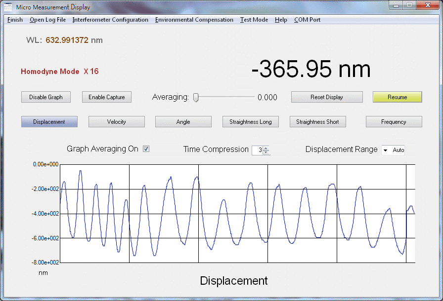
Displacement selects basic measurement of position or distance.
It is probably the mode that will be used most often. The displacement
data is also what all other measurements are based on.
Velocity selects measurement of linear velocity defined as
rate of change of displacement.
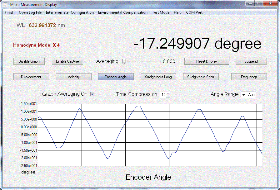
Angle selects angle mode and assumes the use of special
angular interferometer optics, either commercial from HP or similar,
or home-built.
When the "Encoder" checkbox in Interferometer Configuration is checked
µMD2 will use the constant small angle increment WTIHOUT the Trig
calculation and the text will change to "Encoder Angle".
This is useful with rotary encoders and ring laser gyros.
Straightness Long selects straightness mode using long range
straightness optics.
Straightness Short selects straightness mode using short range
straightness optics.
Flatness measurements using the angular interferometer optics with
the 55282A Flatness Accessory Kit (10773A Flatness Mirrors and 10759A
Foot Spacing Kit) should be possible in µMD2
but I have been unable to determine
how exactly it's supposed to work. There is no explicit Flatness
button. Flatness seems to be a linear
deviation based on the combination of the measured angle and foot spacing
dimensions (2, 4, or 6 inches). For small deviations, it may be as
simple as using the Encoder Angle option with a specific Angle Reflector
Spacing value. However, the result would still be in angular units.
Alternatively, using "Straightness Short" with a custom value for
"Straightness Short Coefficient" set to the
ratio of the foot spacing to the angle reflector spacing
may be better. For example,
using the 2 inch (50.8 mm) foot Spacing plate and standard 32.61 mm
10771A Anguler Reflector, the Straightness Short Coefficient would
be set to 1.558, and 3.116 for the 4 inch and 4.673 for the 6 inch.
But for maximum precision, the calculation may need to
be done using an external application like Excel or Matlab operating
on the raw data. However, it would appear that the error for a 1 degree
angle (which would be HUGE) is less than 1 part in 106.
If anyone understands the Flatness measurement, or
has used µMD2 for Flatness, or doesn't agree with these
conclusions - or does, please contact me via email.
Disable Graph toggles whether to show the graph or not and will
change to "Enable Graph" when the graph is off. The data for
the graph is still saved when disabled but certain functions like the
DFT (Frequency) computation are not performed. Disabling the graph
both saves space on the computer screen and reduces computational load.
Enable Capture toggles the acquisition of raw data from the
USB COM port. The log file must first be opened for this button to have
any effect. Then, the label will change to "Disable Capture" and the
button will turn green signifying that capture is enabled and running.
Once the log file is open, capture may be turned on and off at will
with data appended to the open log file. Prior to each segment, the
line "Sample Frequency = XXX.XX Hz" is stored. The Sample Frequency
can be one of several values depending on the laser's REF frequency
and may thus be useful for data analysis (though it is very unlikely
to switch values while using any given laser). Currently the ranges are:
REF less than 1.45 MHz: 457.76 Hz.
REF 1.500 to 1.725 MHz: 610.35 Hz.
REF greater than 1.775 MHz: 732.42 Hz.
The gaps in the REF frequencies are for hysteresis to prevent rapid switching
back and forth if at the border. And if you must know, the reason for
different sample frequencies is to optimize sub-count interpolation.
(If Firmware V60.00 is installed with LowCPUClockEnable set to 1, there
is an additional sample frequency of 305.17 Hz below a REF of 1.075 MHz.)
The ranges are subject to change without notice, but probably not
by much and no one should really care. :)
There are three options to select what data is saved:
For all conditions using interferometer data EXCEPT where the Test Mode
function generator is set to Constant and is OFF, only
Displacement and Sequence Number are saved.
The format is: "D: Displacement N: Sequence Number" where
Displacement and Sequence Number are values in decimal. The Displacement
an integer multiple of wavelength times the multiplier depending on the
type of interferometer. It does NOT include the phase or sub-wavelength
interpolation value. Example:
D: 51643 N: 15345
Assuming the use of a Plane Mirror Interferometer (10706A, basic increment
of 1/4 wavelength), the Displacement would be 51643 * 158.25 nm or
approximately 8.172 mm.
When the Test Mode function generator is set to Constant and OFF,
ALL interferometer data is captured without any annotation.
The format in Single Axis Mode (8 values) is: "REFFrequencyCount
MEASFrequencyCount Displacement VelocityCount Phase SequenceNumber
LowSpeedCode LowSpeedData". Example:
1534 1532 51643 2 144 15345 0 0
The format in Mulitiple Axis Mode (16 Values) is: "REFFrequencyCount
MEAS1FrequencyCount Displacement1 Velocity1Count Phase1 SequenceNumber
LowSpeedCode LowSpeedData MEAS2FrequencyCount Displacement2 Velocity2Count
Phase2 MEAS3FrequencyCount Displacement3 Velocity3Count Phase3".
Where the Test Mode function generator is ON and thus it is desired
to capture the simulated Test Mode data, Axis 1 data is stored.
The format regardless of mode is: "R: REFFreqeuncyCount M: MEASFrequencyCount
D: Displacement V: VelocityCount P: Phase N: SequenceNumber T" where the
"T" signifies that this is Test Mode data. Example:
R: 1534 M: 1532 D: 51643 V: 2 P: 144 N: 15345 T
Caution: The log file can grow rapidly - especially where all the data is
stored - so it's probably not the sort of thing to do for hours on end
unless you have stock in a disk drive manufacturer! :)
All these formats have a fixed number of fields that are space-delimited.
Thus importing the log file into programs like Excel or Matlab should be
straightforward.
Averaging adjust the "strength" of a moving average from 0 (no
averaging) to 999 (1000 samples of averaging). It is a logarithmic
scale so each third of movement represents approximately a factor of 10.
The color also changes from black to violet to remind you that averaging
is taking place. :)
When interpolation is enabled (the default), as averaging coefficient of
around 900 is recommended to minimize sample-sample noise in the graph.
The Averaging coeeficient is saved upon exiting the GUI.
Reset Display zeros the displacement and clears any errors
that may have occurred.
Suspend freezes the readout and graph and the button label
changes to "Resume" and its color changes to yellow. Pressing the
button then restarts the readout and
graph at exactly the point they left off. Thus, any change in position
or other parameter of the interferometer is not detected while suspended.
Suspend is useful when making adjustments to the inteferometer beam path
and/or laser.
Graph Averaging On checkbox determines whether averaging is
also applied the graph. Thus the graph can show raw data even if the
readout is averaged. (Does not apply to Frequency mode.)
Time Compression applies a sub-sampling factor to change the
rate of the graph scrolling. It does NOT average intermediate samples -
they are lost. (Applies to all except Frequency mode.)
The Time Compression factor is saved upon exiting the GUI.
Displacement, Velocity, Straightness Long, and Straightness Short
Range select the vertical axis scaling for their respective modes
including Auto (which is the default).
The format is slightly modified when Frequency mode is selected. This
graphic shows the actual DFT of the triangle waveform in the one above.
Note that the DFT coefficients go as 1/N rather than 1/N-squared because
it's actually using the velocity data, which is a squarewave.
µMD2 Main Window in Frequency Mode with Graphing Enabled
Frequency selects frequency mode which displays the frequency
content of the velocity data up to about 100 Hz on the graph.
(The 0 to 30 Hz range is shown.)
It uses a Discrete Fourier Transform algorithm operating on the
velocity data. Thus, the Velocity button is also highlighted when
Frequency is selected to indicate this. The actual algorithm computes
the power spectral density and takes its square root.
The horizontal scale is approximately accurate for real data. The vertical
scale is somewhat arbitrary. The Main Readout shows Displacement
data when in frequency mode.
DFT Frequency Range determines the span for Frequency mode.
(Does not apply to other modes.)
The DFT Frequency Range is saved upon exiting the GUI.
DFT Amplitude Range selects the vertical axis scaling for
Frequency mode, including Auto (which is the default).
Main Window Indicators
Next are the various fields for displaying information in the Main Window:
µMD2 Main Window Showing Most Indicator Fields
Main Readout always shows the value of the measurement for the
mode that is selected except when in Frequency mode, in which case
it shows Displacement.
The units for the Main Readout, as well as for the graph vertical axis
(all except Frequency mode) are selected in the Interferometer
Configuration window. The options are nm, µm, mm, m, in, and ft for
all but angle, which has arcsec, arcmin, and degree. For velocity,
"/s" is added. The same units also apply to the graph
"Range" selection and vertical axis of the graph.
WL is the wavelength after environmental compensation
(if enabled).
REF is the actual REF frequency of the laser. REF is accurate
to better than 0.5 percent. It will only be present if there is a REF
signal after the laser is READY.
Loss of the REF signal will result in a "REF (Head) Error" if error
detection is enabled. This error may also be forced by clicking on
the REF frequency value.
MEAS is the frequency return signal from the measurement path
of the interferometer. MEAS is accurate
to better than 0.5 percent. It will only be present if a MEAS
signal is present.
Loss of the MEAS signal will result in a "MEAS (Path) Error" if error
detection is enabled. This error may also be forced by clicking on
the MEAS frequency value.
DIFF is the computed difference frequency between REF and MEAS.
DIFF is accurate to better than 0.5 percent. It will only displayed if
both REF and MEAS signals are present.
If the DIFF frequency exceeds valid limits, a "Slew (Rate-) Error" or
"Slew (Rate+) Error" will be generated if error detection is enabled.
These errors may also be forced by clicking on the DIFF frequency value.
Which one will depend on the direction of change of the displacement
at the instant of the click.
Simulated Data will be present whenever the Test Mode function
generator is ON to remind you that it's too pretty (or ugly) to be
interferometer data. :)
Error Detection Off will be present when the Error Detection
checkbox is not checked in the Test Mode window.
Log File displays the name of the current open file for data
capture. The Capture button will only have an effect if a log file
is open.
Phase, PBA RM RP, RMA RM RP, PE, SF Hz, and DP32 % are diagnostic
information for testing purposes. These will only be visible if the
"Diagnostic Readouts" checkbox is checked in the Test Mode window. These
are subject to change without even a femtosecond's notice.
These entries provide for selection of the type of interferometer used for
displacement/velocity measurements, the measurement units to be used
for the Main Readout and graph, parameters for the strightness and
angular optics, and whether to enable use sub-count interpolation.
All interferometer configuration parameters are saved when exiting the GUI.
µMD2 Interferometer Configuration Window
Linear coefficienets:
These settings only affect linear measurements.
LI / Other (1X) is used for the 10702A Linear Interferometer
or other interferometers with a resolution of 1/2 wavelength like the
Single Beam Interferometer (10705A).
PMI (2X) is used for the 10706A Plane Mirror Interferometer,
10706B High Stability Plane Mirror Interferometer, or other interferometer
with a resolution of 1/4 wavelength.
HR PMI (4X) is used with the 10716A High Resolution
Plane Mirror Interferometer or other interferometer with a resolution
of 1/8 wavelength.
Units (as appropriate)
nm, µm, mm, cm, m select Metric units which apply to
displacement, velocity, and straightness measurements in the readouts
and graph.
in, ft select English units which apply to displacement,
velocity, and straightness measurements in the readouts and graph.
arcsec, arcmin, degree select the units to be used for angle
measurements in the readouts and graph.
Known quirk: If neither the COM Port or Test Mode is active, switching
among the Units buttons will only change the Units lable and/move the
decimal point/precision without affecting the readings. Just thought
you should know. ;-)
Parameters (as appropriate):
Angle Reflector Spacing enables the precise spacing parameter of
the angular optics to entered. The default of 36.610 mm is for the 10770A
Angular Interferometer with 10771A Angular Reflector. This
may also be set to some other value to accomodate an angle interferometer
with a different coefficient. (Range 1 to 100 mm in steps of 0.001 mm.)
Straightness Long Coefficient enables the precise multiplier for
the straigntness long interferometer to be selected. The default of 360 is
for the 10775A Long Range Straightness Interferometer with Cal 1.00. This
may also be set to some other value to accomodate an interferometer
configuration with a different multiplier coefficient relative to
displacement. (Range 100 to 1000 in steps of 0.01.)
Straightness Short Coefficient enables the precise multiplier for
the straigntness short interferometer to be selected. The default of 36
is for the 10774A Short Range Straightness Interferometer with Cal 1.00.
This may also be set to some other value to accomodate an
interferometer confirguration with a different multiplier coefficient
relative to displacement. (Range: 1 to 100 in steps of 0.001.) May
also be used for Flatness.
Miscellaneous:
Reverse Polarity flips the sign of the checked
axes. The measured direction of motion depends on the type
of laser (5501A/B versus 5517) and type and orientation
of the interferometer. Applies to all modes and graph. Frequency
will not change in the steady state, but since it uses the velocity graph
data, there will be a transient if the polarity of the primary axis
is changed on the fly.
Encoder Checkbox enables linear angle calculation with respect
to half wavelengths / Angle Reflector Spacing if checked. Useful
for devices like rotary encoders and ring laser gyros.
The combination of the Angle Reflector Spacing and Wavelength then
define the encoder's resolution. The text for angle mode will
change to "Encoder Angle" if the Encoder Checkbox is checked.
This is also equivalent to using the small angle approximation
for angle, but all the time. :)
Interpolation Checkbox enables sub-count interpolation if checked.
Interpolation is implemented in the firmware by computing an estimate of
the relative phase of REF and MEAS. It provides both an increase in
absolute accuracy and in resolution but is only really valid for slowly
changing data. Both are inversely proportional to the laser's REF
frequency. Thus the benefit is less for a 5517D (REF 3.4 to 4.0 MHz)
compared to a 5517A (REF of to 1.5 to 2.0 MHz). As currently implemented,
interpolation should work for lasers with REF frequencies from around
1.1 MHz to 4.8 MHz. Under some unspecified
condition, interpolation may work for higher REF lasers but this is not
guaranteed and errors are not considered bugs. :) It is limited at the
low end by the available CPU registers to store phase samples and at the
high end by the granularity of the CPU clock with respect to the REF
and MEAS counts. If there is a special requirement for interpolation
with a low REF laser like the Optralite (250 kHz), special firmware might be
available.
The accuracy is improved compared to the basic measurement by
approximately a factor of 20 MHz/(the lasers's REF frequency). Thus
a 5517B at 2 MHz with a PMI (basic resolution of 158 nm) would have
an effective accuracy of around 16 nm.
The resolution (defined as a detectable change) may be below
1 nm but there is a slowly varying drift due to the way the
laser's REF and MEAS synchronize with the CPU clock. In fact,
movement below 1 nm is easily visible. For reference, 1 nm is about the
width of 8 hydrogen atoms sitting patiently side-by-side. ;-) We are
working to minimize or eliminate this drift but it may not be easy.
The following graphs are of data from an actual interferometer
with a mirror mounted on a custom built high stability PZT so that small
movement could be programmed from an electronic function generator (e.g.,
Wavetek). Before installing this assembly directly on the Plane
Mirror Interferometer, small programmed movement was totally swamped
by vibrations from the fan of the laptop on which the GUI was running.
And gentle tapping on a table two floors up was easily detectable
in the µMD2 readout and graph (via Remote Desktop).
Note the vertical scale of the graphs. This is unretouched real
data. The PZT is driven by triangle waveforms with p-p amplitudes of 60
and 10 nm for the left and right graphs, respectively. Note that GUI
averaging is also turned on with settings of 900 to
950 (10 to 20 samples) so part of the improvement occurs because of that.
But without interpolation, no movement at all might show up regardless
of GUI averaging setting, since 60 nm and 10 nm are much less than the
basic resolution of 1/4 wavelength using a Plane Mirror Interferometer.
Examples of Actual Displacement Data with Amplitudes of 60 nm p-p (left) and 10 nm p-p (right)
This provides for entry of temperature, pressure, and humidity, or to
select the use of environmental sensor data if available. All environmental
compensation parameters are saved when exiting the GUI.
µMD2 Environmental Compensation window
Note: Temperature, pressure, and humidity values from installed sensors
are currently only acquired when the board is reset, but are sent
periodically to the GUI.
Temperature Value may be entered in degrees C, F, or K as
specified by the Temperature Units Select. Any change results in
the compensation factor being recalculated.
Temperature Units Select may be used to specify degrees C, F, or K.
When selected, the temperature value is reset to 20, 68, or 293
degrees, for C, F, and K, respectively.
Temperature Auto Checkbox enables the use of a temperature sensor
if available. If the Auto checkbox is checked but no sensor is available,
the value will not change.
If the Temperature Auto checkbox is checked, the value sent by the firmware
overwrites the value in the Temperature Value box using units selected by
the Temperature Units Select box. The correction is then recalculated.
Test Mode sends 34 °C.
Pressure Value may be entered in mm/Hg or mBar (hPa) as
specified by the Pressure Units Select. Any change results in
the compensation factor being recalculated.
Pressure Units Select may be used to specify mm/Hg or mBar. When
selected, the pressure value is reset to 760 or 1,000 for mm/Hg and mBar,
respectively.
Pressure Auto Checkbox enables the use of a pressure sensor
if available. If the Auto checkbox is checked but no sensor is available,
the value will not change.
If the Pressure Auto checkbox is checked, the value sent by the firmware
overwrites the value in the Pressure Value box using units selected by the
Pressure Units Select box. The correction is then recalculated.
Test Mode sends 567 mm/Hg.
Humidity Value may be entered in increments of 1%. Any change
results in the compensation factor being recalculated.
Humidity Units Select Only relative humidity is supported.
Sorry, live with it. :) When selected, the humidity value reverts back
to 50 percent.
Humidity Auto Checkbox enables the use of a humidity sensor
if available. If the Auto checkbox is checked but no sensor is available,
the value will not change.
If the Humidity Auto checkbox is checked, the value sent by the firmware
overwrites the value in the Humidity Value box. The correction is then
recalculated.
Test Mode sends 89%.
Wavelength Correction Buttons: turn Environmental Correction on
and off. Changing their state also resets the display. The default is ON
(using 20 °C, 760 mm/Hg, and 50% RH).
Vacuum Wavelength is the nominal wavelength which may be found
in the spec sheet for the specific laser. For reference, the default value
is 632.991372 nm (should it get changed accidentally or otherwise).
Wavelength Correction On and Off determine if environmental
compensation is enabled. The corrected wavelength will be displayed
as WL in the Main Window.
Note 1: With the current GUI, the Factors for Temperature, Pressure, and
Humidity will change either based on the entered values or via the hardware
sensors (if implemented). HOWEVER, their exact value is not guaranteed to
be meningful and should only be considered for trends. This was supposed
to be fixed when the environmental calculations were corrected using the
NIST formulas, but the staff assigned to do the work took a couple years
off, sorry.
Note 2: With Environmental Compensation turned OFF, the vacuum wavelength
is used in calculations. Therefore, Environmental Compensation should
be turned ON even if using standard values.
The primary use of Test Mode is to exercise the GUI without the need for
a laser or actual interferometer hardware. :) The only other user function
that is useful would to disable error detection suring setup and alignment
of the laser and optics.
µMD2 Test Mode Window
Simulated Data On/Off controls the software function generator.
When enabled, its data overrides the data from the USB port. The waveform
is not affected by the Interferometer Configuration.
Waveform - Constant, Ramp, Triangle, Sine select the function.
The Waveform is saved upon exiting the GUI.
Frequency selects the function generator frequency with range
from 0.1 to 1 kHz. The slider increment is 1 percent of the selected range.
The entered frequency for the triangle and sine waveforms roughly
corresponds to real-time but this is not guaranteed.
Amplitude selects the function generator amplitude with ranges
from 0.01 to 1. The slider increment is 1 percent of the selected range.
Offset selects the function generator offset with a range
of +/-1 to +/-100. The slider increment is +/-1 percent of the selected
range.
REF is used as the REF frequency for the function generator
to compute MEAS and DIFF.
The REF value is saved upon exiting the GUI.
Units apply to amplitude with the same options as for the
interferometer - nm, µm, mm, cm, m, in, ft. These apply only
to the output of the function generator and do NOT affect the Main Window
units settings. There are no angle units.
Note that while Test Mode will operate in Angle mode, the values it sends
are linear displacements. Thus, what this really means may be too difficult
for the average human brain to evaluate and may result in an overload
and unintentional brain reboot. :)
The Units selection is saved upon exiting the GUI.
Multiple Axis Mode Checkbox enables the function generator to
send data to any combination of up to 3 axes. When checked, axis select
checkboxes appear below it to enable the selected axes. More on multiple
axis options below.
Axis 1, Axis 2, and Axis 3 checkboxes select the desired
axes for use with the Test Mode function generator.
Error Detection Checkbox enables error detection when checked.
It may be desirable to disable error detection during interferometer
setup or laser testing.
The Error Detection state is saved upon exiting the GUI.
Diagnostic Readout Check box enables the display of up to
four diagnostic values in the Main Window. Not really useful unless
you're doing GUI or firmware development.
The Diagnostic Readout state is saved upon exiting the GUI.
Reset Display replicates the function of the reset button in the
Main Window.
While the firmware handles up to three measurement axes, only limited
support is provided in the GUI due to the software complexity and lack of
demand at the present time. What is present should be enough to get
started. It's possible this could chenge in the future but don't hold
your breath in anticipation. It may never happen.
If the GUI detects data (MEAS clocks) on axes 2 or 3, the firmware and GUI
enter Multiple Axis Mode utilizing an expanded communications format, and
the appropriate readouts will appear as shown below.
µMD2 Main Window with Multiple Axes Active
All GUI functions apply to the primary axis, which defaults on startup
to Axis 1. The primary axis is what the Main Readout, REF/MEAS/DIFF
frequency displays, frequency analysis, averaging, and graph
apply to. Clicking on the Axis 1, Axis 2, or Axis 3 labels will
select it to be the primary axis and change the color of the selected
axis label to identify it as the primary axis. The units of the primary
axis are also used for the others. Error detection (if enabled)
only applies to the primary axis. Averaging is NOT applied to the
Axis 1, Axis 2, or Axis 3 readouts, even the one that is the same as
the primary axis.
Note that in Multiple Axis Mode, the communications format sends somewhat
more data over the USB COM port and the GUI must perform more computation.
Thus this may cause problems for a wimpy pre-Jurassic PC operating on
the hairy edge of what's possible. Once Multiple Axis Mode is entered
using the interferometer hardware, the only way to return to Single Axis
Mode is to restart both the firmware and GUI. This is because neither has
any way to know whether dropouts of measurement clock signals are due to
a beam path being momentarily interruprted or an axis actually being shut
off (whatever that might mean).
Test Mode is also capable of exercising all three axes singly or in combination
but the function generator data will be the same for all. This is controlled
by the Multiple Axis Mode checkbox. When enabled, Axis 1, Axis 2, and
Axis 3 checkboxes will appear below it with Axis 1 being the default
on startup. Turning Multiple Axis Mode off will put the GUI back in
Single Axis Mode. But this will be overidden when Test Mode is turned
off if the USB port is enabled and the firmware is running with multiple axes.
Multiple Axis GUI support is currently under development. Specifications and
behavior are subject to numerous changes without notice. ;-) However, no
major features beyond what are described above are anticipated to be
implemented in the GUI.
Help Menu
Information has only one purpose at present: To direct you to
this µMD2 Installation and Operation Manual! ;-)
µMD2 Information Window
About lists the GUI build and firmware versions, and provides links
our (Jan and Sam) Web sites.
µMD2 About Window
Troubleshooting
Naturally, all is expected to go smoothly. But if it doesn't, here are
some common problems. Some of these may be bugs in the firmware or GUI
as hard as that is to believe. So, if you find something that cannot
be solved based on what's below, contact us for a timely response:
GUI won't start and generates error about value out of range:
Ignore the error by hitting "continue" as there is no configuration file. The
GUI should come up. Close it using "Finish" and it will save a valid
configuration file and the error will not appear again except possibly
if a new GUI Build is run since each one has a unique configuration
file. (This error should not occur but at least be prepared!)
GUI starts but then generates error about value out of range:
If you are in a location where the interpretation of "." and "," differs
(e.g., Brazil), numbers with decimal points may get screwd up. One specific
instance is that for the wavelength in the Environmental Compensation window,
the decimal point gets ignored so that 632.993172 is interpreted
as 632991372, which is obviously out of range. Sorry, you'll just
have to move your entire operation to the USA (or at least set the
environment that way for now). ;-)
There is no valid USB Port available: The firmware is not running
or has crashed. (Hard to believe!) Exit the GUI and assuming the firmware
has been loaded, press the RESET button. With the present firmware, after
about 1 second, LED3 should be on at reduced brightness when the firmware
has started. It's actually flashing at the sample frequency but this may
not be obvious except by waving your eyeballs.
GUI generates error when the USB Port is selected: This means
either the firmware is not producing the proper communications sequence
or more likely, the board has simply gotten out of sync. Selecting the
USB Port a second time will usually clear it.
Graph is not scrolling after USB Port is selected: Similar to
above. First try selecting the USB Port again, but may require exiting
the GUI, pressing RESET, and reatsrting the GUI. Attempting to run
with an incompatible version of the firmware or firmware not properly loaded
or in a peculiar state can also produce this error.
There is no change in displacement even when there should be:
Assuming the REF and MEAS are coming from the correct sources (laser and
optical receiver, respectively), this usually means the interferometer
is installed or assembled incorrectly (e.g., backwards), is misaligned,
or the laser is not producing the proper F1/F2 optical signals.
Displacement takes off up or down out of control: In most cases,
MEAS (down) or REF (up) is simply missing. If the laser isn't READY, the
there will be no REF signal. If the interferometer isn't set up or the
measurement path is blocked or misaligned, there will be no MEAS signal
sporadically or all the time. Either the REF or MEAS frequency readout
will be blank. Unless errors are disabled, usually this should result
in a "Hd Error" (no REF) or "PA Error" (no MEAS). The first thing to do
if the problem isn't obvious is to swap the REF and MEAS connectors.
If the error also swaps, then there is a problem with the signal from the
laser or optical receiver; if the error stays the same, the problem is
in the wiring or line receiver.
In rare cases, such behavior can be due to a noisy REF or MEAS signal as a
result of crosstalk or improper termination. The REF or MEAS frequency
readouts will differ significantly even with no movement and will not be
accurate for the noisy signals(s). If a 50 MHz or higher bandwidth
oscilloscope is available, check the quality of the REF and MEAS signals.
REF and MEAS(s) should not be run together for long distances without separate
shielding. And while the default value of 150 ohms for the terminating
resistors is generally satisfactory, depending on your wiring run length
and other factors, using a different (probably lower value) may be necessary.
Substituting a UA9639 for the UA9637 (if used) may also help.
It is a slower part and will tend to filter out any glitches. This
wouldn't be a preferred solution though and might earn you an "F" in
my CSE371 Intro to Computer Design course. :( :)
Due to the way the PIC synchronizes the Timer inputs (which includes REF
and MEAS) with the CPU clock, a glitch can manifest itself in peculiar
ways, possibly only causing problems at specific sample frequencies (which
are based on the CPU clock frequency).
Displacement or velocity values are off by an integer factor: The
Interferometer Configuration does not match you interferometer hardware.
Angle or Straightness values are not accurate: The parameters of
your interferometers are non-standard. They may be adjusted over a wide
range in Interferometer Configuration.
Displacement wonders by a few nanometers over seconds: Due to the
way sub-count interpolation is implemented, there is an unavoidable (for now)
artifact due to the relative sampling of the REF and MEAS signals and the
CPU clock. Sorry, µMD2 Research is spending sleepless nights on
this problem. (Also applies to other measurements.) You have a really
stable physical setup if you can even detect this issue! ;-) µMD2
Research had to attach a mirror on PZT directly to a 10706A Plane Mirror
Interferometer for it to appear.
Update of GUI readouts and other indicators is sporadic or slow:
While µMD2 should run on just about any computer that still runs,
this cannot be guaranteed for a 20 year old machine. Time to Upgrade.
However, CPU intensive applications like antivirus scans can hog resources.
The USB subsystems on some computers are more efficient than others and
there's no way to predict performance based on make or model.
Sensor values are not updating in real-time: Even if installed and
enabled, presently, they are only acquired just after the firmware is reset
and are NOT sent continuously. So, this is feature, not a bug. :)
Using µMD2 GUI with Homodyne Interferometers
Note that the standard µMD2 firmware does NOT support homodyne operation
(either not well or not at all). A special version is available and it has
no warranty whatsoever. :) See below.
While originally designed and optimized for heterodyne interferometers using
two frequency HP/Agilent/Keysight and similar lasers, the µMD2 GUI can
also be used with homodyne (single frequency)
interferometers. The interferometer optics used with these systems are
identical to those for two-frequency lasers, but the electronics
typically provide baseband SIN/COS "quadrature" outputs rather
than REF and MEAS frequencies. For use with µMD2, the analog
signals must be converted to digital pulses to increment or decrement
the displacement counters. In fact, other measurement instruments
providing quadrature signals like those using high resolution optical
encoders can also be used with µMD2.
Firmware may use the SG-µMD2 board
or an even less expensive platform like the Atmega 328 Nano 3.0. (Under
$3 on eBay.) However, without some minimal additional quadrature decoding
hardware, performance will be severely limited with either.
As long as the communications format is adhered to, the µMD
GUI will interpret
displacement correctly. So, rudimentary firmware would accept SIN/COS
quadrature signals thresholded to TTL levels
to increment or decrement displacement, resulting in
up to 4 counts per cycle or a resolution of around 79 nm with a
Linear Interferometer (LI). (but with the Interferometer
Configuration set to 4X.) There is no sub-wavelength interpolation
option. However, a quad-pulse converter (4 counts/cycle)
multiplies the resolution by a factor of 4 compared to the same optics
with a two-frequency laser. So using a Plane Mirror Interferometer (PMI)
would result in a native resolution (no interpolation)
of just under 40 nm. These values come about from (1) 2X from
the optical path up and back, (2) 2X from the PMI, and (3) 4X from the 4 counts
per cycle of the quadrature decoder. With a
High Resolution PMI, the resolution becomes ~20 nm. And some commercial
metrology laser systems provide increased resolution via interpolation
internally. But even the basic resolution of ~40 nm is not too shaby. ;-)
However, since the counting
must be done in real-time, the uninterruptable portions of the USB
serial data handler are a serious limitation for implementations not
using a hardware pulse converter and counter. By minimizing the size of
the unused values to reduce the time spent in the serial communications,
this can be somewhat improved but it's still not pretty. Using the Atmega 328
Nano 3.0 with a PMI, the speed is currently limited to less than 1 mm per
second, and some GUI functions like Velocity and Frequency won't do anything
useful. Inquire for a copy of this Atmega firmware if interested in hacking
it. ;-)
With minimal external logic to convert the SIN/COS quadrature to digital
quadrature and then to TTL pulses, this speed
limitation would virtually disappear using the Teensy 4.0
with its
internal counters. A PLD, discrete logic, commercial chip like the LS7083
"Encoder to Counter Interface", or even another microprocessor like the
Atmega, would generate UP and DOWN pulses based on the SIN/COS signals.
More modern versions of SIN/COS interpolator chips are available with
multiplications factors of up to thousands (though at limited
speed), though output edge rates of many Mhz are possible depending
on the interpolation factor.
UP would increment the REF counter and DOWN would increment
the MEAS counter. Their difference would then be the Displacement just
as in the standard µMD2 firmware. Data would be sent at a fixed sample
rate of 732.42 Hz and all GUI functions would be supported. A second
measurement channel would use the other two counters. The internal counters
can run at over 20 MHz, so perfomance would be limited mostly by the speed
of the optical receiver and quad-to-pulse converter.
A hardware implementation for the converter would provide the highest
performance. However, depending on the actual requirements,
there may be no need to dust off those old TTL chips or PLD programmer.
When using a $2 Atmega 328 Nano 3.0, the maximum speed was
measured to be order of 40 kHz for each of 2 channels using quick-and-dirty
polling using the pathetically slow Arduino digitalread and digitalwrite
instructions. With a few minutes of optimization invoking direct PORT
calls instead, the aggragate throughput went up to order
of a million (X4) counts/second. That's about 4 cm/sec with a PMI.
Substituting a second Teensy 4.0 or PIC32MX250F128B board
(chipKIT or SG-µMD2) to be used only for the converter should result in
a several fold improvement over that.
There is a version of the µMD2 firmware
that supports homodyne mode with 1 or 2 channels each using pairs of internal
counters (>20M counts/second max but requiring an external pulse
converter to generate the up/down pulses), along with a third
channel via direct polling of Quad-A-B digital inputs.
The maximum speed of the third
channel is under 350 counts/second but this could still be useful for
some applications like the Z axis in a high resolution 3-D
printer. ;) To accomodate non-interferometer measurements using
optical or mechanical encoders, the entry for "Vacuum Wavelength" in
the "Environmental Compensation" window (632.991372 nm for HP/Agilent
lasers) has a range of 1 nm to 1,000,000 nm (1 mm) so it can be set
to the appropriate resolution required for anything from
an atomic force microscope to a construction crane. ;-) If a value
outside this range is required, contact me. ;-)
To display rotation angles from optical encoders (or ring laser gyros)
properly, there is now an option in the GUI to bypass the non-linear
calculation required by the Angular Interferometer. With the "Encoder"
checkbox in the Interferometer Configuration screen checked, the
the angle will read correctly based on the Angular Reflector Spacing
being the radius of the encoder and the wavelength being (X4) count
spacing around the periphery.
The graphic below shows µMD2 being used to test a home-built
ring laser gyro. It is being rotated by hand on a Lazy Susan turntable.
Screen Shot of Sam's RLG Angle Readout using µMD2
Interpolation for higher resolution is possible using the raw SIN/COS
analog signals and often done in commercial systems.
However, I have absolutely positively no intention of
even thinking about any implementation using the existing µMD2 hardware.
And as noted, the basic resolution using a single frequency HeNe laser and
PMI with quad-A-B digitally thresholded signals is under 40 nm. With a
HiRes PMI, it would be under 20 nm. If you need something better then
that, you probably have a budget to go with it. ;-)
Summary of homodyne inputs for µMD2 (chipKit DP32 or SG-µMD2
    Pin    Signal   Counter   Function         Maximum Speed
 -----------------------------------------------------------------
   0/RB5    RPB5    Timer3    Axis 1 Up    >20M counts/second
  11/RB0    RPB0    Timer5    Axis 1 Down       "          "
  13/RB2    RPB2    Timer4    Axis 2 Up         "          "
  14/RB3    RPB3    Timer2    Axis 2 Down       "          "
  10/RA1    RPA1      --      Axis 3 A     350 transitions/second
  18/RA4    RPA4      --      Axis 3 B          "          "
To achieve higher performance from a less expensive platform like the
Atmega, an external up/down counter could also be added, which would
be read by the firmware via the digital inputs.
Support for homodyne interferometers is currently a "works-in-progress"
so nothing is currently polished in the same way as µMD2 for
heterodyne interferometers. :)
Quad-A/B to up/down converters
For most of these schemes, the quadrature-A/B (digital) inputs must be
converted to up/down pulses to increment or decrement the counters that
represent displacement. Here are several possibilities:
The first one is a discrete TTL implementations.
Aynchronous Quadrature to Pulse Converter
should run at 5 MHz or more. But there are a pair of discrete delays and the
relative propogation delays of the 74LS04s and 74F153 are critical
which may be just as bad as using monostables (which would earn you
an "F" in my logic design course).
With some tweaks, the maximum speed can be greatly increased and this
would fit into a small PLD or FPGA.
The next one uses an inexpensive Atmega 328 Nano 3.0:
Atmega sketch:Single_Channel_Quad-Pulse_fw_v06. This uses direct port calls.
Replicate code (with obvious changes) for additional channels.
This provides up to a three channel Quad-A/B to pulse converter
using the Atmega 328 Nano 3.0. Two channels could be used
with the µMD2 chipkit DP32 counters and firmware below.
This should work on other similar
Arduino-compatible platforms. It also provides a cool demo of
quad-to-pulse conversion if LEDs (with resistors) are put on the
input and output pins (below). :) Aggragate throughput 0.5 to 1 mpps
(all channels) using polling (no interrupts) with direct PORT access
(bypassing the sluggish Arduino libraries).
Atmega sketch:Quad-Pulse-Demo_fw_v03. This is ONLY for a demo if LEDs (with resistors) are
attached to the output pins.
Having said all that, here is the good stuff. :) It has been tested with
a Renishaw RLE10 Fibre Optic Encoder with an RLD PMI head. In "Coarse"
mode, it has the basic homodyne resolution of ~40 nm (1/16th wavelength).
RLE10 "Fine" mode provides an additional 4X interpolation internally
so the native resolution (with no interpolation in µMD2) is ~10 nm
(1/64th wavelength). Pathetic. ;-)
Homodyne firmware and GUI
The following Beta version chipKit DP32/SG-µMD2 firmware
and GUI supports homodyne operation with two high speed axes (pulse
up/down) and one low speed axis (quad A-B) using the above pin assignments.
The "#define Homodyne" statement near the top of the firmware should be
set to the desired number of homodyne axes
- which really should not be greater than 1 at least at first - I don't
know if 2 or 3 axes work correctly. :( :)
The "#define HomodyneMultiplier" statement near the top of the firmware
should be set to the integer number of counts/cycle for
the encoder hardware - most commonly 4 using a quad pulse converter.
However some commercial systems provide various modes with higher
resolution. For example. the Renishaw RLE "Fibre-Optic Encoders" have
Coarse and Fine modes. Coarse is 4X while Fine is 16X for a displacement
resolution of around 10 nm with a PMI. The latest GUI automagically knows
about the homodyne resolution so the type of interferometer will be all
that needs to be specified. This does not affect Test Mode behavior.
The "define V10_PCB" near the top of the firmware should be set to
1 ONLY if using the SG-µMD2 V1.0 PCB LED6 (chipKit LED3).
All it affects is the LED. Maybe.
Although V59.01 also includes the heterodyne code, IT IS NOT GUARANTEED
to work correctly and any bug fixes since the homodyne branch
may not have been included, so unless you are a total masochist and
want to reconcile differences between v59.01 and the latest heterodyne
firmware, it should only be used for experimenting with
homodyne interferometers. But if running it results in
the Universe imploding, I do not want to know about it. ;-)
For this version of the firmware, LED3 indicates
the percentage of time spent in the processing and communications
routines in a ~3.2 second cycle as follows:
Processing (PRC): ~0.8 s.
Short gap, off: ~0.4 s.
Communications (COM): ~1.2 s.
Long gap, off: ~0.8 s.
The brightness of LED3 on chipKit (LD6 on SG-µMD1) is
proportional to the time spent in PRC or COM.
If it is full on or full off continuously, something bad probably happened.
GUI: The latest version of the GUI (in the section:
Latest Versions of the GUI, above) should work
with a single homodyne channel but may need some "minor"
tweaks to deal with 2 or 3 channels. Inquire if interested. If you
ask nicely, I may be inclined to provide the GUI source code. ;-)
Else the minor tweaks that µMD Tech Support doesn't consider
fundamental errors may not be completed until well beyond the end
of time.
When the COM port is selected with homodyne firmware, the GUI will
display "Homodyne Mode" followed by "X" and the Multiplier (counts/cycled
specified in the firmware "#define HomodyneMultiplier" statement) on the
main screen. The frequency counters are blanked and most errors
are disabled.
This has been tested with a Renishaw RLE10 Fibre Optic Encoder with an RLD
PMI head with the Atmega-based quad to pulse converter. Using the RLE10 "Coarse" mode, it has the basic homodyne resolution
of ~40 nm (1/16th wavelength). Using its "Fine" mode provides an additional
4X interpolation internally so the native resolution (with no interpolation
in µMD1) is ~10 nm (1/64th wavelength). Pathetic. ;-) The graphic below shows
an approximately ±400 nm change in displacement at 10 nm resolution
from just gently pushing down on the optical breadboard with the PMI head
and planar mirror mounted on a micrometer stage.
But the micrometer is way too crude for nm-scale movement.
Screen Shot of Test of Renishaw RLE10 Fibre Optic Encoder using µMD2
There may be a high performance version of the homodyne hardware and firmware
in the future. Stay tuned but don't hold your breath. :)
Where performance is a total non-concern, here is a low speed
Quad-A/B USB interface for the µMD2 GUI using the Atmega 328 Nano
3.0 ONLY (no chipKit at all). Three channels should be possible
with performance of up to around 350 pps on each one:
Atmega firmware:Atmega
µMD0 Firmware v03. This is an early single channel version.
It's incomplete and probably doesn't even compile but should provide
the general idea when
compared to the normal µMD2 firmware. If you are inclined to
make this work, I may consider assisting. :)
But I have no intention of putting µMD2 on an ATTiny. ;-)
Using µMD2 for DIY LIGO?
The Laser Interferometer Gravitational wave Observatory (LIGO) uses what
is basically a very special (and expensive) Michelson interferometer
to detect gravitational waves emanating from colossal cosmic events
millions of lightyears distant. A Web search will find many publicly
aavailable references. Its sensitivity to changes in the position
of its mirrors is order of 1/1,000th the diameter of a proton or
about 1 attometer, 1x10-18 meters. That's about 1,000,000,000
times more sensitive than µMD2 with a Plane Mirror Interferometer.
So perhaps not. ;-) (But the cost was much greater also!)
However, it would be possible to demonstrate the principles of LIGO as well
as to add some of the enhancements to boost sensitivity like extending
the reference arm and adding multi-pass cavities on both arms. A
Single Beam Interferometer (PBS cube and 2 QWPs) might be used along with
a pair of high quality mirrors in each arm to multiply the effective path
length and sensitivity.
At the very least, such a setup would be a very sensitive earthquake detector,
though detecting black hole or neutron star collisions is out, unless they
occur in our Solar system (which would probably be bad). ;-)
The Future
As of Fall 2017, the chipKIT DP32 is no longer available from Digilent,
though until Winter of 2019, it was still available direct from microchip
as part number TDGL019. But now it appears to be certifiably gone and
although Digkey sent me a "laser time buy" email on it, I rather doubt
that's meaningful. And I've exhausted availability from all other
distributers.
If you already have the chipKIT board or ordered µMD2, this
isn't a real concern unless you are planning to duplicate your setup at a
later date or would like a spare just in case something bad happens.
In that case, getting another chipKIT DP32 board would make sense.
I have purchased enough of these to handle anticipated
demand for the next year or so, but a longer term solution is now
called for. But the number is going down fast.
There are several options for the µMD project going forward:
Design a custom PCB that would provide the functions of the chipKIT
DP32 along with the line receivers, connectors, and environmental
sensors. The PIC, or an equivalent, should continue to be available
for the foreseeable future, though it may eventually need to be an SMT
version. I have a monitor placed on microchip's "end-of-life" watch
should the PIC32MX250F128B-I/SP (the 28 pin DIP version) be scheduled to go
out of production. Then I could just buy up a lifetime supply. :)
Laying out a PCB is no problem, but this approach would
also require having the boards assembled (stuffed with parts and soldered),
programmed, and tested.
Switch over to another PIC-based Arduino compatible board.
The recommended replacement for the chipKIT DP32 is the
Digilent µC32. However, the µC32 appears to NOT
have some of the essential features required for µMD2 - notably
external clock inputs to the the Timers. And a separate widget board
"Shield" would need to be added for the "peripherals" and both the cost
and complexity is therefore somewhat greater.
For this to be viable, the PIC must have a minimum of 4 high speed counters
(microchip calls them "Timers") whose clock inputs can be configured to
connect to external pins. Surprisinigly, most PIC32 parts even in packages
with many more pins do not have this capability.
Redo µMD2 using a different microprocessor or FPGA. (µMD2!)
A possible solution is the
Cypress CY8CKIT-059 PSoC®
5LP Prototyping Kit With Onboard Programmer and Debugger. This
has a microprocessor with FPGA so it
could be an opportunity to greatly boost performance including support
for lasers like the Zygo 7701/2 which have a 20 MHz REF frequency, along
with better sub-wavelength interpolation and potentially even support
for closed-loop control.
Needless to say, this would be a very complex undertaking and the
justification may simply not be there. Only a small number of
hobbyist/experimenter types even care about the sub-wavelength
interpolation, let alone Zygo support. And I have no intention of
developing µMD2 for serious commercial release.
I have already begun (1) and prototypes are now available. Parts have also
been ordered. This PCB includes the layout for the
line receivers and environmental sensors as well as most other chipKIT
features except for the EEPROM (though there is space for it). It's all
through-hole except for the USB Micro B connector, which can be either
through-hole or SMT. This project will proceed, but with enough chipKIT
DP32 boards in stock for awhile, there should be a smooth transition.
The only downside to this approach for the user is that I do NOT intend
to populate the PCBs, even for basic PIC32 functions. So a bit more soldering
is involved. See the specific info in the section:
If someone were interested in working with Jan and myself on (2) or (3)
(or some other option not listed),
please contact me via the link at the top of this page. However, I have
no current plans to do (2) or (3) on my own.