Optical Receiver 3 (OR3) Gain Options

Version 1.00 (16-Nov-21)

Copyright © 1994-2022
Sam Goldwasser and Jan Beck
--- All Rights Reserved ---

For contact info, please see the Sci.Electronics.Repair FAQ Email Links Page.

Reproduction of this document in whole or in part is permitted if both of the following conditions are satisfied:
  1. This notice is included in its entirety at the beginning.
  2. There is no charge except to cover the costs of copying.

Summary

Here are three minor variations of OR3 depending on maximum gain (or sensitivity). Generally, the fully populated PCB can be used for any optical input power (and it also has a low and high gain setting based on the jumper on JP1). Reducing the gain may be useful in a noisy environment or to simplify construction. However, in most cases, everything here can be ignored. ;-)

  1. Low Gain Version: Eliminate and bypass Gain Stage 2. Jumper the lower two pins of JP1:

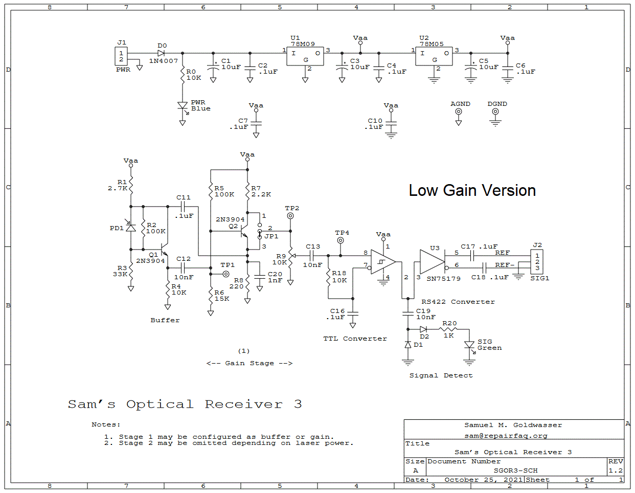
    OR3: Low Gain Schematic

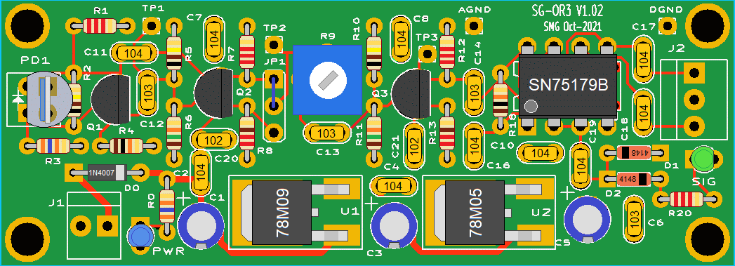
    OR3 Low Gain Component Locations

    .

  2. Medium Gain Version: Eliminate and bypass Gain Stage 2. Jumper the upper two pins of JP1. This is the one that should work for most applications.

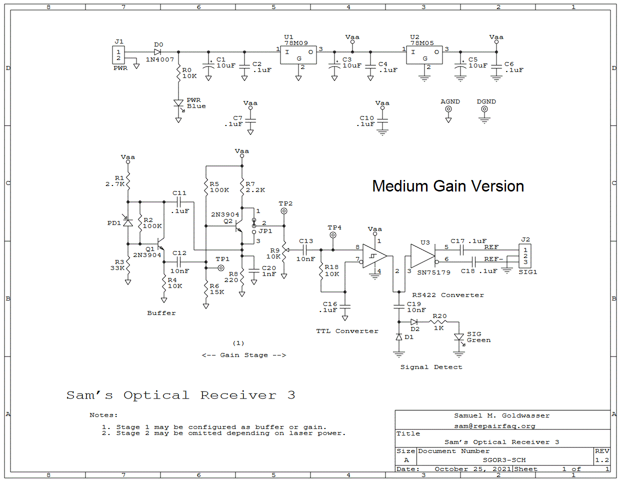
    OR3: Medium Gain Schematic

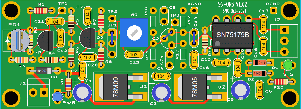
    OR3 Medium Gain Component Locations

    .

  3. High Gain Version: Jumper the upper two pins of JP1. Installation in a shielded case may be required to avoid interference from other sources.

    This is the same as the default schematic except for the jumper. It can also be set up similar to the medium gain version by jumpering the lower pins of JP1.

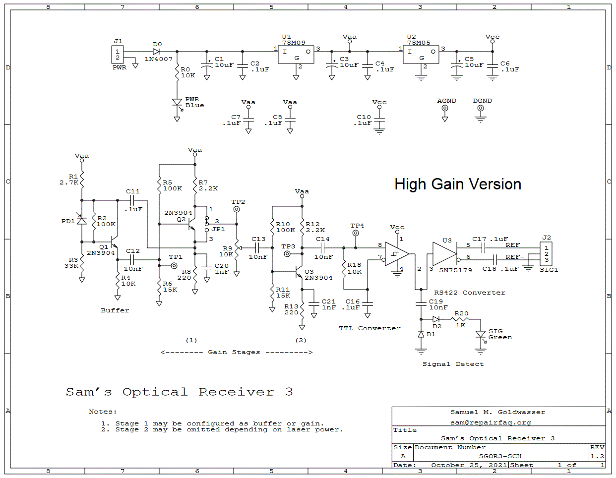
    OR3: High Gain Schematic

    OR3 High Gain Component Locations

    .