All Rights Reserved
Reproduction of this document in whole or in part is permitted if both of the following conditions are satisfied:
1. This notice is included in its entirety at the beginning.
2. There is no charge except to cover the costs of copying.
DISCLAIMER
SG-AB is intended for use in hobbyist, experimental, research, and other applications where a bug in the hardware will not have a significant impact on the future of the Universe or anything else. We will not be responsible for any consequences of such bugs including but not limited to damage to the wafer FAB you picked up on eBay for $1.98 + shipping, financial loss from the use of 37 spools of ABS due to the office 3-D printer fabricating a part 25.4x too large in all dimensions, or bruising to your pet's ego from any number of causes directly or indirectly related to SGAB2. ;-)Introduction
Note: Local links and clickable graphics open in a single new tab or window depending on your browser's settings.Homodyne interferometry and optical encoders require conversion from the optical detectors to so-called Quad-A-B signals. At low speed, this is not much more than a photodiode with load resistor and digital comparator. And parts like that are included in the various interferometer and entry-level displacement masurement systems. But such a simple scheme is limited to a few thousand counts per second - perhaps up to a few 10s of thousand of counts per second - but not the performance needed for most real applications. For example, to track motion at 1 cm/s using a plane mirror interferometer would require more than 60,000 counts/second (where 1 c/s is equivalent to 1 Hz).
The purpose of the Quad-A-B Preamp (henceforth referred to as QAB2 or simply AB2) is to provide a simple solution that accepts photodiode inputs and generates differential RS422 A and B signals that can be input to µMD0, µMD1, µMD2, or another compatible displacement measuring system. This is not the ultimate device as it is strictly digital Quad-A-B not analog Quad-Sin-Cos. Nor does it have support for an intensity channel to accomodate a varying input amplitude. Those capabilities may come in the future, but don't hold your breath in anticipation. ;-)
QAB2 is on a 1.6 inch by 2.25 inch PCB and runson 12 to 15 VDC. (The PCB itself is called SG-AB2.) The optical input is a beam up to ~3 mm in diameter (using the default photodiode) with an optical power from <25 µW to >1 mW. The actual photodiodes may be mounted up to a few inches from their pads on the PCB but coax or twisted pair should be used beyond that where noise pickup may be a concern. QAB2 has >3 MHz bandwidth (full cycle) which is more than adequate for systems using the kit lasers as well as for many real applications. With a Linear Interferometer which has a full cycle of ~316 nm, the slew rate can be greater than 1 meter per second, which is a fairly nutty velocity. ;-). And it is expected that the bandwidth limit can be extended with trivial changes to only a few part values. This is left as an exercise for the student. ;-)
The actual SG-AB2 PCB is four layers with internal power and ground planes.
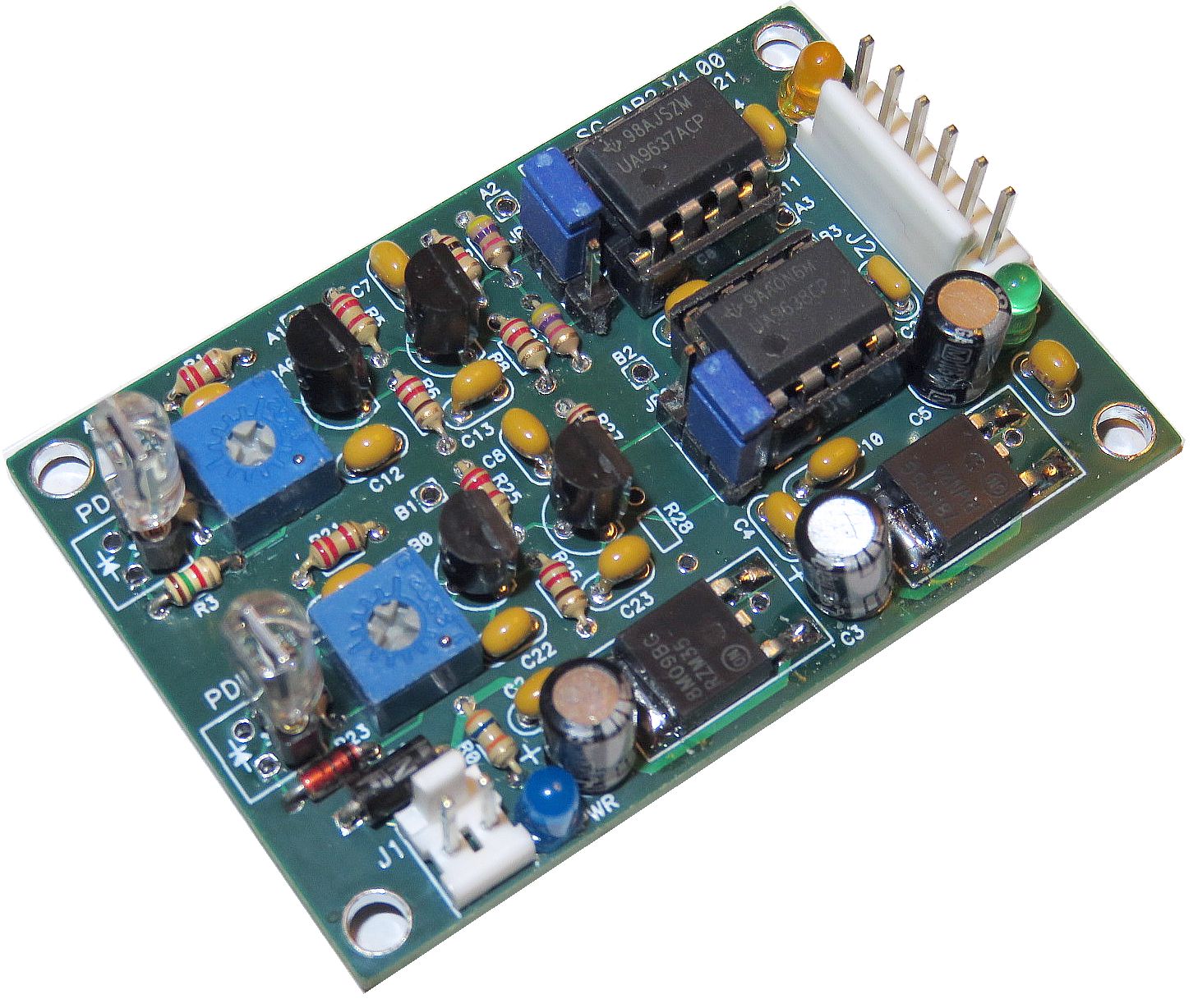
Populated AB2 V1.00 PCB
And yes, a careful examination will show that a couple parts do not match the schematic or layout, below. Some experimentation is underway, and there is a minor "oops". ;-) More on that later. And I was all out of red LEDs, so the A SIG LED is orange for the photo. ;-)
While the photodiodes are shown plugged into sockets on the PCB, in actual practice, they will likely be on the quad decoder PCB with short cables connecting them. This was for testing. A companion quad decoder PCB for the photodiodes is planned, though the QD1 PCB can be used with minor modifications.
Specifications
- Laser compatibility: Commercial and home-built single frequency
HeNe lasers as well as multi-longitudinal lasers
(not single frequency) if the Path Length Difference
(PLD) between the REF and MEAS beams including traversals through
the interferometer optics is less than a few cm.
- Bandwidth: 0 to >3 MHz. It is probably usable at more than
4 MHz but testing was done using my 1-3 MHz variable REF laser as a signal
source.
- Sensitivity: Less than 25 µW up to 3 MHz,
less than 15 µW at 1 MHz. Lower level inputs may be
used but at some point QAB2 will
need to be installed in a shielded box so that the local AM radio station
isn't picked instead of the optical signal. :( :) There values are the
optical power incident on the linear polarizer.
- Adjustment: Trim-pot to set mid-point threshold.
- Number of channels: One each for A and B. The only difference
between them is the color of the LED to show high or low signal. ;-)
- Inputs: Silicon photodiodes in sockets or soldered directly.
- Signal indicators: Red (A) and green (B) LEDs.
- Outputs: 6 pin header (compatible with µMD2)
or screw terminal block for RS422 A/A-, B/B-, and GND.
- Power: 12 to 15 VDC at less than 150 mA. Where slightly
lower frequency response is acceptable, the 78LM09 can be replaced
with a 78M05 with the 78M05 bypassed so the input could be as low
as ~7 V or both IC regulators may be omitted and bypassed so that
QAB2 can run on 5 VDC directly. For optimal
performance, the bias resistors may need to be tweeked
for voltage lower than 9 V on the analog parts. This is left as an exercise
for the student. ;-)
- PCB: 1.6 x 2.25 inch four layer board with mostly
through hole components. Only the two voltage requlators are surface mount.
- Firmware, software, GUI: None. ;-)
Parts List
Note: There are gaps in some part number sequences by design. ;-)
 Prt  Description                  Comments
-------------------------------------------------------------------------
  -   PCB, SG-AB2 V1.00            First released version

  D0  Diode, 1N4007 or similar     Reverse polarity power protection

  C1  Capacitor, 10-22 µF          Input power bypass
  C2  Capacitor, 0.1 µF            Input power bypass
  C3  Capacitor, 10-22 µF          +9 Vaa bypass
  C4  Capacitor, 0.1 µF            +9 Vaa bypass
  C5  Capacitor, 10-22 µF          +5 Vcc bypass
  C6  Capacitor, 0.1 µF            +5 Vcc bypass
  C7  Capacitor, 0.1 µF            +9 Vaa bypass
  C8  Capacitor, 0.1 µF            +9 Vaa bypass
  C9  Capacitor, 0.1 µF            +5 Vcc bypass
 C10  Capacitor, 0.1 µF            +5 Vcc bypass
 C11  Capacitor, 0.1 µF            PDA feedback or bypass
 C12  Capacitor, 1 nF              1st stage A frequency compensation
 C13  Capacitor, 1 nF              2nd stage A frequency compensation

 C21  Capacitor, 0.1 µF            PDB feedback or bypass
 C22  Capacitor, 1 nF              1st stage B frequency compensation
 C23  Capacitor, 1 nF              2nd stage B frequency compensation

  R0  Resistor, 36K, 1/8 W         PWR LED current limiting

  R1  Resistor, 2.2K, 1/8 W        1st stage A power
  R2  Resistor, 10K, 1/8 W         1st stage A bias
  R3  Resistor, 1K, 1/8 W          PDA load
  R4  Trim-pot, 1K                 PDA load trim
  R5  Resistor, 2.2K, 1/8 W        1st stage A collector load
  R6  Resistor, 220, 1/8 W         1st stage A emitter load
  R7  Resistor, 2.2K, 1/8 W        2nd stage A collector load
  R8  Resistor, 220, 1/8 W         2nd stage A emitter load

  R9  Resistor, 2.2K, 1/8 W        RS422 receiver threshold
 R10  Resistor, 2.2K, 1/8 W        RS422 receiver threshold

 R11  Resistor, 220, 1/8 W         LED A current limiting
 R12* Resistor, 10K, 1/8 W         2nd stage A base current limiting

 R21  Resistor, 2.2K, 1/8 W        1st stage B power
 R22  Resistor, 10K, 1/8 W         1st stage B bias
 R23  Resistor, 1K, 1/8 W          PDB load
 R24  Trim-pot, 1K                 PDB load trim
 R25  Resistor, 2.2K, 1/8 W        1st stage B collector load
 R26  Resistor, 220, 1/8 W         1st stage B emitter load
 R27  Resistor, 2.2K, 1/8 W        2nd stage B collector load
 R28  Resistor, 220, 1/8 W         2nd stage B emitter load

 R31  Resistor, 2.2K, 1/8 W        LED B current limiting
 R32* Resistor, 10K, 1/8 W         2nd stage B base current limiting

  U1  LM78M09, IC, Regulator, 9V   Vaa 9 V regulator (SMT)
  U2  LM78M05, IC, Regulator, 5V   Vcc 5 V regulator (SMT)
  U3  IC, UA9637                   RS422 receiver
  U4  IC, UA9638                   RS422 driver

 PDA  Silicon photodiode           Optical sensor A
 PDB  Silicon photodiode           Optical sensor B

 PWR  LED, blue                    Power LED
  A   LED, red or orange           A LED
  B   LED, green                   B LED

  Q1  Transistor, 2N3904           1st stage A (impedance matching)
  Q2  Transistor, 2N3904           2nd stage A (gain)
  Q3  Transistor, 2N3904           1st stage B (impedance matching)
  Q4  Transistor, 2N3904           2nd stage B (gain)

  J1  Header/shell/pins or Screw   Power input
       terminal block, 2 pin

  J2  Header/shell/pins or screw   Signal output
       terminal block, 6 pin

  J3  Header/shell/pins or screw   For photodiode A if attached with cable
       terminal block, 2 pin

  J4  Header/shell/pins or screw   For photodiode B if attached with cable
       terminal block, 2 pin

 JP1  Jumper block, 3 pin          Gain select A
 JP2  Jumper block, 3 pin          Gain select B

 SKT1 Socket, 8 pin                For UA9637
 SKT2 Socket, 8 pin                For UA9638
 SKT3 Socket, 2 pin                For PDA if installed directly
 SKT4 Socket, 2 pin                For PDB if installed directly
For those not familiar with the common resistor color code (Black/0, Blown/1, Red/2, Orange/3, Yellow/4, Green/5, Blue/6, Violet/7, Gray/8, White/9), the resistors shown above are 150 ohms (brown-green-brown or 15 with 1 zero) ohms and 330 ohms (33 with 1 zero) ohms. The gold stripe indicates 5 percent tolerance on the value but for the use here, tolerance doesn't matter. (It's possible the resistors you use will have 4 stripes where 3 of them are the value and the 4th is the multiplier, along with one for tolerance. If in doubt confirm the value with a multimeter.) The chart below is from Digikey. (If the link decays, a Web search will readily find another one.)

Resistor Color Code Chart (from the Digikey Web site)
All of these resistors are 1/8 watt which are a bit tiny. So, use a bright light and magnifying glass if necessary as it's easy to confuse locations and color of the bands. If in doubt, measure the resistance with a DMM. As they say in woodworking: "Measure twice and cut once". Replacing a part is much more difficult and risky than installing the correct one in the first place!
The direction of the resistors doesn't matter though it is good practive to have them line up with the labels on the PCB. The polarity of the diodes, electrolytic (large value) capacitors, and the photodiode IS critical. Refer to the layout diagram, above.
The yellow ceramic capacitors are labeled on one side with two digits (always "10" for the values used in QAB2) and a multiplier as power of 10: 102 (1,000 pF, 1 nF), 103 (10,000 pF, or 10 nm), or 104 (100,000 pF, 100 nm, 0.1 µF). The diodes are labeled in itty-bitty print.
Schematic for the QAB2 Version 1.0
The schematic for QAB2 is shown below. (Schematic version numbers are not the same as PCB version numbers.)
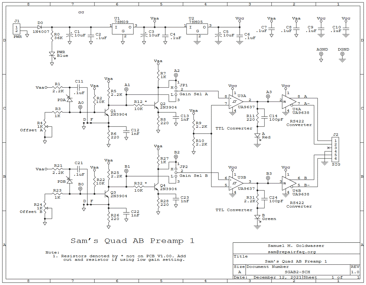
QAB2 Version 1.0 Schematic
The graphic below shows the general appearance of the PCB with most of the parts installed:
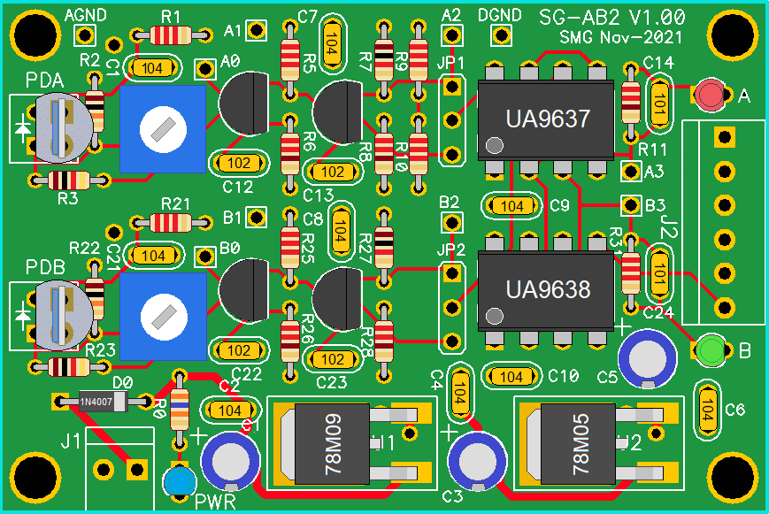
SG-AB2 PCB Version 1.00: Location of most Components
Printing out the schematic and having it available for reference while assembling the PCB may be helpful.
Assembly
As promised, here are the detailed "Heathkit™-style" instructions for assembling the SG-AB2 V1.00 PCB.All components are through-hole except for the voltage regulators (U1 and U1), and except as noted in the detailed assembly procedure, should seat flush on the PCB. They shouldn't be suspended in mid-air swinging in the breeze. :) The resistors in particular like to not stay flat on the PCB unless their leads are bent at a steep angle. Most components are identified on the silk-screen and with only a few exceptions, the label won't be obscured when the part is installed.
A low power soldering iron with narrow tip and thin (e.g., #22 AWG) rosin-core solder will be required. DO NOT even think about attempting this without suitable soldering equipment. It's well worth the investment. A Weller soldering gun or propane torch will not work. :) Rosin core solder is also essential. And while I'm quite confident that you never make mistakes, a means of component removal such as a de-soldering pump (e.g., a full size SoldaPullt™) will be highly desirable. Screwing up component removal can easily ruin the PCB and is not covered under the limited unlimited warranty. :-)
Proper soldering technique will be such that the exposed solder on each pad should be shiny with a concave profile. It should not be a blob and just needs to fill the hole. Solder is not glue. Some excess solder doesn't hurt anything but looks unprofessional. A 10X magnifier may come in handy for inspection. Residual rosin can be cleaned off with isopropyl alcohol or an environmentally-friendly electronic solvent. However, leaving the rosin alone is also acceptable (if ugly).
Total assembly time should be well under 1 hour for someone proficient in fine soldering. Cutting component leads to 1/4 to 3/8 inch before installation will simplify soldering as the long leads won't be poking you in your one good eye. :( :) Then trim flush after soldering.
Print out this document so each step can be checked off ( ) as it is completed.
The parts list below assumes populating with with all components. Exceptions will be noted.
- ( ) Confirm that all parts are present and undamaged:
- ( ) 1x blank SG-AB2 V1.00 PCB. Confirm the version on the
silkscreen. Inspect for plating or other defects.
- ( ) 3x 10 or 22 µF electrolytic capacitor.
- ( ) 9x 0.1 µF ceramic capacitor (marked 104).
- ( ) 4x 1 nF ceramic capacitor (marked 102).
- ( ) 4x 100 pF ceramic capacitor (marked 101).
- ( ) 5x 220 ohm 1/8 W resistor (red-red-brown).
- ( ) 4x 1K ohm 1/8 W resistor (brown-black-red).
- ( ) 6x 2.2K ohm 1/8 W resistor (red-red-red).
- ( ) 4x 10K ohm 1/8 W resistor (brown-black-orange).
- ( ) 1x 36K ohm 1/8 W resistor (orange-blue-orange).
- ( ) 2x 1K ohm trim-pot (marked 102).
- ( ) 1x 78M09 IC regulator.
- ( ) 1x 78M05 IC regulator.
- ( ) 1x UA9637 IC RS422 receiver.
- ( ) 1x UA9638 IC RS422 driver.
- ( ) 2x Photodiode.
- ( ) 1x Blue LED.
- ( ) 1x Red or orange LED.
- ( ) 1x Green LED.
- ( ) 4x 2N3904 transistor.
- ( ) 1x 1N4007 or similar diode.
- ( ) 3x 2 pin header with shell and pins or screw terminal block.
- ( ) 1x 6 pin header with shell and pins or screw terminal block.
- ( ) 2x 2 pin male-to-female socket strip.
- ( ) 2x 8 pin DIP socket.
- ( ) 2x 3 pin jumper block and jumper.
Inspect the parts closely, especially the (yellow) ceramic capacitors as they may all be physically identical. The labeling is TINY and easy to read incorrectly. It's also easy to misread the itty-bitty 1/8th watt resistor color bands. In some cases, slighlty different values for resistors may be included such as 30K in place of 36K, but these should be intuitively obvious. ;-)
Testing of the LEDs inserted into the PCB but prior to soldering is recommended. They are very fragile the leads are stressed while soldering. Bend the leads out at a small angle so the LED stays in place and cut them short but DO NOT solder until thee LED has been confirmed to work. Then without stressing the leads, solder quickly and retest.
Double check the part value before soldering. Use a magnifying glass if necessary. As they say in carpentry: "Measure twice and cut once.". Even with proper desoldering equipment, removing a part without damage to either the part or PCB can be dicey.
Parts denoted with "+" below may be omitted if only the low gain version is needed (for input optical power above ~100 µW).
- ( ) 1x blank SG-AB2 V1.00 PCB. Confirm the version on the
silkscreen. Inspect for plating or other defects.
- ( ) Correction for design error (GASP!): This is needed if using
the low gain (bottom) jumper position with the 2nd stage components installed
because the Offset Adjust trim-pot may not have enough range.
It isolates the base of the 2nd stage so its input
has a greater voltage swing. Please refer to
SG-AB2 PCB Modifications for
Low Gain. Cut the 4 traces on the component side of the PCB denoted
by "Xs" in yellow and add the 2 jumpers (also in yellow) and 2 10K ohm
resistors (R12+ and R32+) on the bottom of the PCB.
- ( ) Install U1 (LM78M09 voltage regulator). This is most easily done
by adding a tiny bit of solder to the lower-right pad and then holding
the chip in place while heating that leg on the IC. Then solder the
upper right leg, and finally the tab with just enough solder to form a
continuous bead along its length.
- ( ) Install U2 (LM78M05 voltage regulator) in a similar manner.
- ( ) Install J1 (2-pin header or screw terminal block). For the header,
the plastic tab faces toward the center of the PCB. For the terminal
block, the wire access holes face out.
- ( ) Install PWR (blue LED). The longer lead goes toward the center
of the PCB and the flat goes toward the edge. See note above with
respect to soldering LEDs.
- ( ) Install D0 (1N4007 or similar diode). Pay attention to the polarity.
- ( ) Install R0 (36K ohms, oranage-blue-orange).
- ( ) Install C1, C3, C5 (10 µF). Note polarity: Positive is marked on the PCB and is also the square pad. Negative on the capacitor is the line.
- ( ) Install C2, C4, C6 (0.1 µF).
- ( ) Carefully inspect for solder and component lead shorts and unsoldered
leads. Correct as needed.
- ( ) Smoke test #1. :) Connect a source of 12 to 15 VDC to J1. Pay
attention to polarity. The blue LED should come on and the far right
legs of U1 and U2 should have voltages very close to +9 VDC and +5 VDC
on them, respectively. And nothing should smoke. ;-)
- ( ) Install C7+, C8+, C9, C10 (0.1 µF).
- ( ) (Optional) Install C11, C21 (0.1 µF). When installed
in the default location (F on the schematic), these provide positive
feedback to partially cancel out the photodiode capacitance and may help with
high frequency signals. Since the feedback gain is less than 1, the
system is still unconditionally stable. They can also be installed
as a decoupling (bypass) capacitor to GND (D on the schematic) to an
unmarked nearby GND pad (at a 45 degree angle, sorry). If none of
this makes sense, just ignore it. ;-) Or try them and see if either
is beneficial. Then report your findings. ;-)
- ( ) Install C12, C13+, C22, C23+ (1 nF).
- ( ) Install C14 C24 (100 pF).
- ( ) Install R1, R5, R9, R10, R11, R21, R25, R31 (2.2K ohms, red-red-red).
- ( ) Install R2, R22 (10K ohms, brown-black-orange).
- ( ) Install R3, R7+, R23, R27+ (1K ohms, brown-black-red)
- ( ) Install R4, R24 (1K ohms trimpot, marked 102).
- ( ) Install R6, R8+, R11, R26, R28+ (220 ohms, red-red-brown).
- ( ) Install A and B (red or orange and green LEDs. The longer lead goes
to the left and the flat goes to the right. See note above with respect to
soldering LEDs.
- ( ) Install JP1, JP2 (3-pin jumper block). The jumper shold be placed on
the top position for high gain (less than around 100 µW of beam power)
and bottom position for low gain (greater than around 100 µW of beam
power). These may be omitted and replaced with a jumper wire if the desired
position is known.
- ( ) Install Q1, Q2+, Q3, Q4+ (2N3904 transistor). Pay attention to the
outline on the PCB. These will not seat flush but 1/8-1/4" off the PCB.
- ( ) Install SKT3, SKT4 (2 pin male-female
socket strip) XOR J3, J4 (2-pin header or screw terminal block).
Although the PDs can be soldered directly, the use of the socket
strips is recommended as the photodiodes are nearly as sensitive to failure
due to heat from soldering as the LEDs. Further, for QAB2, it is likely
to make more sense to mount the PDs on the QD1 PCB, not on the SG-AB2 PCB
using a short cable. Therefore, the use of the screw terminal blocks
or headers makes more sense.
Note that there are two possible adjacent locations depending on the polarity of the PD. The one toward the center of the PCB can be used with the face of the PD pointing away from the PCB. Or the other one can be used if the PD is folded over. The anode of the PDs included in the kit is the left pin facing the front with its legs down.
If screw terminal blocks or headers are installed, they should use the outer pair of pins so as to not bump up against R2/R22. A photodiode can still be used with the screw terminal blocks but it will have to face down for the polarity to be correct.
- ( ) Prepare the photodiodes. Depending on the method used to convert
the output of the interferometer to quadrature signals,
Linear Polarizer (LP) or Circular Polarizer (CP - QWP+LP) film may be
attached directly to the faces of the PDs. If installing the PD on the
SG-AB2 PCB in the socket strip (as recommended), the leads can be cut
to a length of ~1/8 inch. But as noted, they will generally be installed
on the QD1 PCB or some other means directly at the output of the
inteferometer. The wires between AB2 and the PDs should be minimized - a few
inches at most as twisted pairs.
- ( ) Install J2 (6-pin header or screw terminal block). For the header,
the plastic tab faces toward the center of the PCB. For the terminal
block, the wiring access holes face out.
- ( ) Install SKT1, SKT2 (8 pin socket). Pay attention to orientation.
To keep these in place while soldering, it is simplest to bend two
corner pins over.
- ( ) Plug U3 (UA9637) and U4 (UA9638) into their respective 8 pin sockets.
Pay attention to notch or dot. Confirm that all pins are seated properly in
the socket. These parts can be damaged if installed incorrectly.
- ( ) Carefully inspect for solder and component lead shorts and unsoldered
leads correct as needed.
- ( ) Smoke test #2: Apply power. Due to the settings of the trim-pots
and hysteresis of the RS422 receivers with no signal, the A and/or B LEDs
may be on. And nothing should smoke. ;-)
- ( ) Initial Operational test: A constant source of light will be required.
This can be a non-Zeeman laser or flashlight on max. ;-)
- As a rough guide for installing the jumper on JP1 and JP2, if the
laser power incident on the photodiodes is expected to be greater
than around 100 µW, use the lower position. Otherwise use the upper
position.
- Apply power. ;-)
- Upper position: Adjust the Threshold trim-pots so their
associated A and B LEDs just go out. Apply your light source to each
of the photodiodes. The associated LED should go on.
- Lower position: Adjust the Threshold trim-pots so their associated A and B LEDs just go on. Apply your light source to each of the photodiodes. The associated LED should go off. (This assumes the "Oops" mod was performed in the second step above.
- Upper position: Adjust the Threshold trim-pots so their
associated A and B LEDs just go out. Apply your light source to each
of the photodiodes. The associated LED should go on.
For an AC test, an LED flashlight with multiple brightness settings may suffice as they usually use PWM to control brightness. An oscilloscope is highly desirable as well since the A and B LEDs can only show that something is there but not what it looks like. The signal could be from a local AM radio station! ;( :)
The idaal threshold settings will be at the mid-point of the sinusoidal optical signal from the interferometer.
- As a rough guide for installing the jumper on JP1 and JP2, if the
laser power incident on the photodiodes is expected to be greater
than around 100 µW, use the lower position. Otherwise use the upper
position.
Theory of Operation
For each channel, QAB2 consists of an impedance matching stage, 1 stage of amplification, a differential-to-TTL converter, TTL-to-RS422 converter, and LED driver circuit as follows:
- The input (1st) stage is modeled loosely on that of the HP-10780 but using
a common 2N3904 BJT in place of the hard-to-find JFET. The 2N3904 is
remarkably capable for a 25 cent (or less) part, with a bandwidth of 250 MHz.
The only change to the circuit is that the BJT needs to be biased into the
conducting state (via R2). This stage acts as a buffer for the photodiode
which is a low current source and also provides a gain of approximately 10..
C11 provides positive feedback to partially cancel the photodiode capacitance.
Since the feedback gain of the emitter follower is less than 1, it is
unconditionally stable.
- The 2nd stage either provides an additional gain of approximately ~4.5x
or is bypassed depending on the position of the jumper, JP1.
- The signal at this point is analog but may be clipped depending on
the selected gain and optical input. The RS422 receiver of the
UA9637 acts as a differential-to-TTL converter. Its specs allow for
the input signal to exceed the normal operating range as long as the
current is limited, which it is in this case to less than 1/5th the
allowable value. The trim-pot (R4) sets the bias point so that the
signal at the UA9637 with no light at the photodiode is just below
the threshold.
- The TTL output of the UA9637 goes to the A or B LED via a current
limiting resistor bypassed with a 100 pF to compensate for the LED's
capacitance.
- The TTL output also goes to the UA9638 driver which provides the RS422 signal to the µMD or other measurement device.
Note that since the gain and voltage drops of transistors is affected by temperature, the threshold may drift a bit as the PCB reaches thermal equilibrium. Sorry. Live with it or wait for the next version which will probably use op-amps which should be mostly immune to drift. ;-) But don't hold your breath in anticipation. I imagine this one will be good enough for most users so it won't happen any time soon.
Troubleshooting
Troubleshooting? What troubleshooting? ;-) Check for solder bridges and unsoldered leads, that the correct parts are installed, and for those with polarity, that they in the right way around. The LEDs die easily damaged from stress during soldering as noted above - at least twice! So, if the Power or Signal LED doesn't light, it may just be a bad LED. The most likely cause of low or no sensitivity is an incorrect resistor value somewhere - it's easy to accidentally misread the color bands. The parts are reliable, though the UA9637 and UA9638 may fail if plugged in backwards or if the 5 V regulator isn't regulating.Beyond this, an oscilloscope will be desirable to be able to trace the signal. There are several strategically placed test-points for this purpose.
For friendly tech support, feel free to contact me via the link at the top of this page. ;-)