Creating RS274X Gerber Files for PCBs Designed using
"Tango PCB for DOS" 
Version 1.05 (12-Dec-21)
Copyright © 1994-2021
Sam Goldwasser
--- All Rights Reserved ---
For contact info, please see the
Sci.Electronics.Repair FAQ
Email Links Page.
Reproduction of this document in whole or in part is permitted
if both of the following conditions are satisfied:
- This notice is included in its entirety at the beginning.
- There is no charge except to cover the costs of copying.
Table of Contents
This document outlines ways to generate RS274X Gerber files
PCBs created with the pre-Jurassic but fabulously wonderful
layout program: "Tango PCB for DOS". (Much of this information also
applies to other ancient PCB layout programs that generate Gerber files
in the RS274D format.) This is the original version of Tango
PCB and has sufficient capabilities for doing quite complex PCB layout
as long there something fancy is required like parts at funny angles
or controlled-impedance traces. And it has a user interface that
results in an experience has been likened to "playing a musical
instrument". I have created 11 x 13 inch 12 layer PCBs using Tango PCB for DOS
in the early 1990s on a 100 MHz Pentium PC running Window 98
in a DOS shell. They had hundreds of
mixed through-hole and SMT components and over 5,000
holes. (No, I didn't route every trace by
hand. Tango sold a separate autorouter which also ran under DOS that
did much of the work, though subsequent cleanup of jiggly and errant
traces was needed.) Subsequent releases of Tango
(after the company were acquired by OrCad) converted to run
under Windows 2000 and beyond have suffered from the limitations of
the Windows GUI as well as creeping featurism on a grand scale. If
you are familiar with Tango PCB for DOS, you know what I'm describing.
If you're not, unfortunately, the program requires a parallel port security
dongle and cannot
be installed from the Web or anywhere else. Or at least, I haven't
figured out a way. I could also not get Tango PCB for DOS to run
under DOSBOX (Note 6) even with its dongle plugged into a valid parallel port.
I'm optimistic that DOSBOX-X will get around this.
And copies of Tango PCB for DOS with the dongle
are now scarcer than raw dragon's eggs and probably
being hoarded as I've yet to find one anywhere. If anyone has more
info on any of this (or one to sell as I'd like a spare), please
contact me via the Sci.Electronics.Repair
FAQ Email Links Page.
The problem with Tango PCB for DOS is that it is only capable of generating
Gerber files in the equally ancient RS274D format which is not accepted by
most PCB houses nowadays including JLCPCB (Note 5). Thus conversion to
RS274X is required. While how to do such a conversion is probably intuitively
obvious to someone who designs PCBs on a daily basis, if just dusting off
"Tango PCB for DOS" every other blue moon,
the following could prove useful. It was
written specifically with JLCPCB in mind but should apply to most others.
This procedure requires Gerbview (Note 1) or another program that can do
RS274D to RS274X conversion. Gerbview is not freeware but offers a 30 day
free evaluation license. And the purchase cost for a single seat license
is relatively modest and justifiable if you want to stick with Tango PCB
for DOS and do a steady stream of PCBs. ;-)
Since Tango is used to generate RS274D-format Gerbers, its
CAM settings are critical:

Some other values work but not all.
The example below is for a 4 layer PCB named 4LAYER.PCB in Tango.
With obvious modifications, it should also apply to PCBs with 2 signal layers
and no plane layers or more than 4 signal layers with or without plane layers.
- Make sure the apertures are set and then generate the Gerbers for
4LAYER.PCB in Tango PCB. Use the extensions: gto, gts, gtl, g1, g2, gbl,
gbs, gbo, and gko for the keepout/board layer. Note: Tango PCB may capitalize
them, which is irrelvant. It will also not maintain the 2-letter g1 and
g2 extensions and will rename them to g10 and g20. Rename them back to
g1 and g2 manually.
- Generate all the Gerber layers and
the Excellon drill file for 4LAYER.PCB using the settings shown
above - ASCII: None and Zero Suppression: None. The typical extension
is .XLN. This is NOT the DRL file that Tango normally produces,
which is just a map of drill symbols and useless for machines.
- Generate the Report (REP) file with the Apertures enabled. It is
needed to convert to RS274X.
- Use Tango's built-in Gerber viewer to do a first pass confirmation that
there are no screwups. There are some things Tango gets confused about,
one example being anomalos edits of polygons. These will show up correctly
in the PCB file but may have extra "doo-dads" in the Gerbers. :( :)
- Load all Gerbers generated by Tango for the 4LAYER.PCB, the drill layer
(4LAYER.XLN), and report file (4LAYER.REP) into Gerbview (Note 1).
- Confirm that all layers including the drill layer show up and are
correct. At this point, PWR and/or GND plane layers are the NEGATIVE of
how they will actually be for production.
- Convert to RS274X as separate files without extensions so they will have
the original extensions. (Clear the extension field in the Conversion
dialog box.) Only "Include old extension as part of new file name" should be
checked. Use a new destination folder so the next step can be completed
without conflict.
- Rename the "_extensions" to ".extensions". E.g., 4LAYER_GTL to 4LAYER.GTL.
- Zip all layers (gto, gts, gtl, g1, g2, gbl, gbs, gbo, drl) along with
a README if desired.
(Two layer PCBs with signal and plane layers may also be possible but normally
the plane layers ONLY include pads for components that are connected to the
plane and there appears to be no way to get Tango to include the others.
So those component leads cannot be soldered unless the signal layer
is on the bottom and then component insertion becomes tricky. PCB gurus
probably have a workaround but I do not know what it is. Playing with
the settings in Tango didn't seem to do anything useful. Thus these
are not recommended. Use a 4 layer PCB instead even if one signal layer
and one plane layer are blank.)
Two layer PCBs can also be done using the procedure, above, and that is
preferred due to known and unknown quirks in TangoKiCAD.
But this one does not require RS274D to RS274X conversion using Gerbview
as KiCad (Note 3) generates RS274X Gerbers directly. However, it can ONLY
be used for PCBs with 1 or 2 signal layers as TangoKiCAD chokes on anything
more complex including more than 2 signal layers and any plane layers.
The example below is for a 2 layer PCB named 2LAYER.PCB in Tango with
signal layers ONLY. (One layer can have nothing on it but must be present
so that there will be pads to solder to on both sides.)
- All that is needed is the Tango PCB file, 2LAYER.PCB saved as ASCII.
Tango is not used to generate the Gerbers.
- Use TangoKiCAD (Note 2) to convert 2LAYER.PCB to 2LAYER..BRD. Only the
source (Tango PCB file) and destination (KiCAD BRD file) fields need to
be filled in. Run "Convert PCB" and exit - TangoKiCAD screws up and may
generate random extra traces (or worse) if run more than once even if the
Tango PCB file is unchanged. TangoKiCAD also has other quirks such as
flipping vertically-oriented text and
deleting polygons and pads that aren't associated with components. (To
include mounting holes and polygons on the PCB, a component with them
must be created.) So carefully double check the PCB in KiCAD for
anomalies. (And to be even more annoying, TangoKiCAD may turn
off "Show window contents while
dragging" for no justifiable reason. To re-enable it, go to "Control Panel,
"System and Security", "System", "Advanced System Settings", "Performance
Settings", and check the appropriate box.)
- Open 2LAYER.BRD with the KiCad Pcbnew editor. No editing needs to be done
except possibly to move the PCB inside the KiCad template (though this
probably doesn't matter). Generate the Gerbers for the top and bottom
layers (gtl, gbl), top and bottom soldermasks (gts, gbs), top and bottom
overlay/silkscreen (gto, gbo), keepout layer (called eco2 in KiCAD, BRD in
Tango), and the drill layer (drl, which is NOT derived from the DRL layer
normally generated by Tango, but from the pads definitions in the PCB
file itself). Rename 2LAYER.eco2 to 2LAYER.gko. The default font for
text in KiCAD may also be different than in Tango.
- Zip all layers (gto, gts, gtl, gbl, gbs, gbo, drl) along with a README if
desired.
Use Gerbv (Note 4) or Gerbview to display the final Gerber
files to confirm that there are no screwups. (Gerbv seems
to be better for viewing and the setup can be saved.) Do this first with
the set you have or will be uploading to JLCPCB. For Plane layers,
set the display to negative in Gerbv by right-clicking on their name(s) on the
left side and selecting "Invert Colors" to show how they will actually be
made. They should appear as mostly copper (negative of what
Tango displays). Once uploaded to JLCPCB, view the
Gerbers in the "Production File" (under the folder "ok") and confirm
again. Plane layers should appear as mostly copper without using the
"Invert Colors" option. Access to the Production Files may require
that the board be paid for and, uh, in production. But perhaps
there's a way to have JLCPCB give you a sneak peak before approval.
Note that I have seen subtle differences in how the layers are displayed
between the Gerbers uploaded and those in the production files "ok"
folder, which are mostly evident when viewed stacked up,
though nothing that should be significant. There may also
be subtle differences between the appearance in Gerbv and
Gerbview due to how they render the layers.
The examples below show the typical appearance of the Gerbers for
a signal layer, a (split) plane layer as generated in Tango PCB, and
the same plane layer from the JLCPCB production file for the board
as displayed using Gerbv.
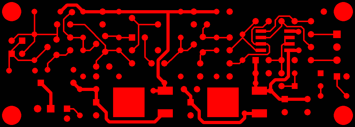
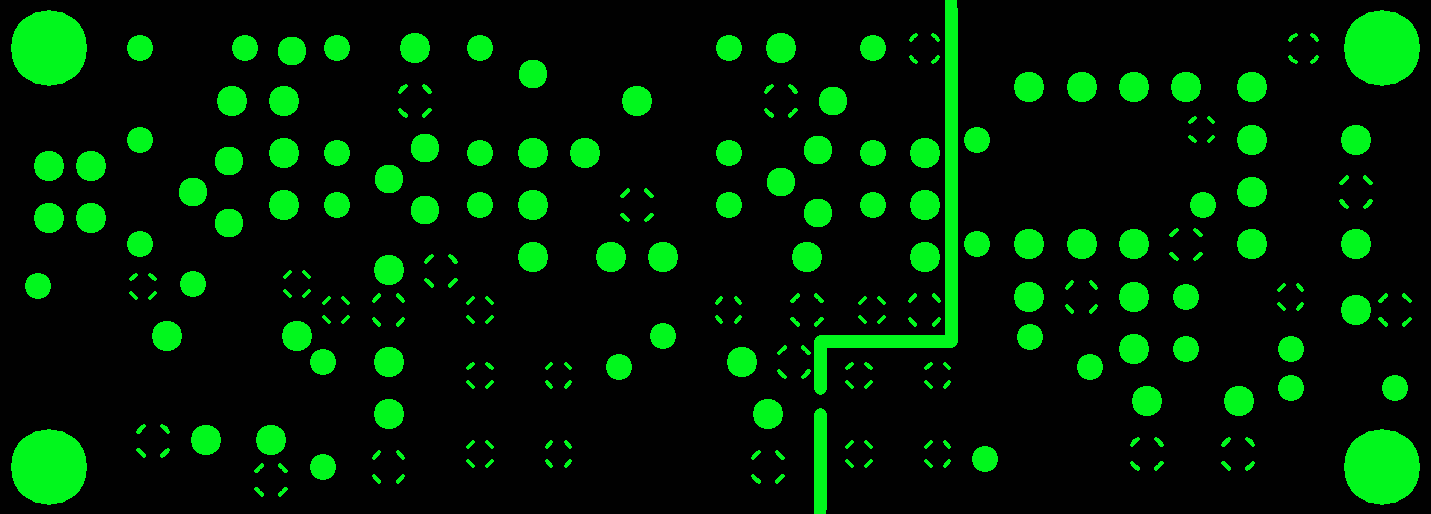
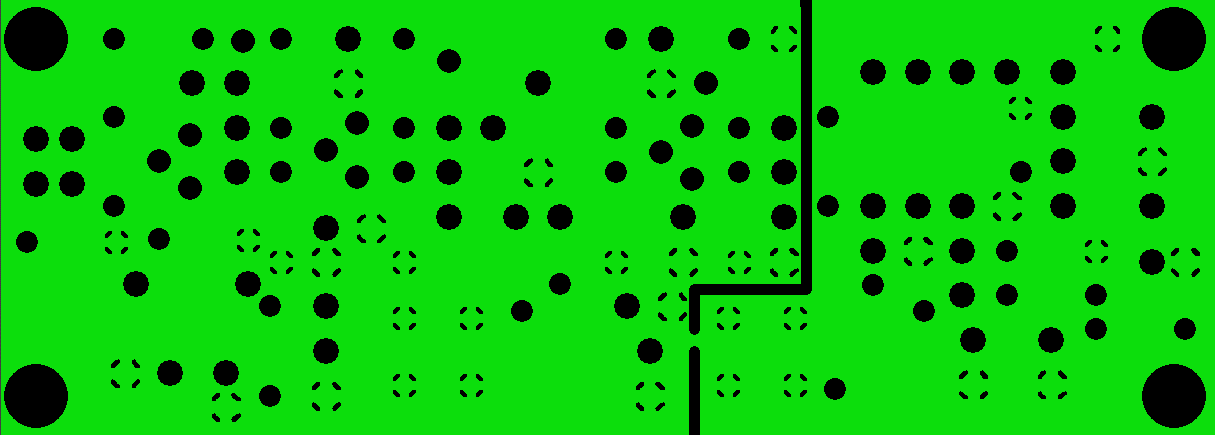
Typical Gerbers: Signal Layer (left, copper is red); Plane Layer
Generated by Tango (center, copper is black); Plane Layer from
Production File (right, copper is green)
- Gerbview is not
freeware but does offer a 30 day free evaluation. Gerbview is useful for
both viewing of Gerbers (both RS274D and RS274X) and conversion from
RS274D to RS274X.
- TangoKiCad seems to have disappeared from the Web. I can provide a copy,
but note that Zonealarm has sometimes believed it to be Malware and deleted or
quarantined it. However, that hasn't happened for several years and I have
never had problems with TangoKiCad for even more years,
except for how brain-dead it is - only supporting PCBs with two
signal layers, screwing up if invoked more than once without
restarting, and messing with the Windows setting "Show window
contents while dragging", (probably among other things). :( :-)
- KiCad is freeware which
includes a suite of CAD tools including a Gerber viewer, though only the PCB
editor is used here.
- Gerbv
is freeware and works well for displaying Gerber files in RS274X format.
Only the Gerbv.exe file is required to display Gerbers. To save and
recall "Projects" (Gerber layer files, stackup, colors, etc.), the
Tiny
SCHEME Init File is required and should be placed in the same folder as
Gerbv.exe.
- JLC PCB is of many
companies that will fab PCBs in small quantities at excellent prices.
I have been very satisfied with their PCB Quality and technical support.
- DOSBOX is a DOS
emulator that runs under modern Windows. While "Tango PCB for DOS" will
attempt to startup in DOSBOX, it aborts since its security dongle is not
recognized. However, there is now a newer version called
DOSBOX-X which is much
more powerful. I'm optimistic that it can be configured to recognize
the "Tango PCB for DOS" dongle. ;-) Stay tuned.