For corrections/comments/suggestions, please contact me via the Sci.Electronics.Repair FAQ Email Links Page.
Copyright © 1994-2001
All Rights Reserved
Reproduction of this document in whole or in part is permitted if both of the following conditions are satisfied:
1.This notice is included in its entirety at the beginning.
2.There is no charge except to cover the costs of copying.
In most cases, this will identify bad silicon transistors. Gain, frequency response, etc. are not addressed here. While the tests can be applied to germanium devices, these are more likely to change characteristics, it would seem, without totally failing.
It is also possible to determine the lead arrangements of identified diodes and bipolar transistors as well as breakdown voltage ratings.
Curve tracers are pieces of electronic test equipment similar to an oscilloscope. They can not only test transistors and other devices but evaluate the functional specifications as well. The chapter: "Curve Tracer Design" includes information on their basic principles of operation and provides details on some very additions to conventional scopes to add some basic curve tracer capability.
This document evolved from a posting on the USENET newsgroup: sci.electronics (no longer active - closest replacement in the sci.electronics hierarchy is probably sci.electronics.components) from Randy Fromm (Randy@randyfromm.com) who maintains a Technical Department with an extensive collection of repair related information.
Before touching, probing, or unsoldering any component, make sure the equipment is unplugged and any large capacitors have been safely discharged. See the document: Capacitor Testing, Safe Discharging, and Other Related Information or the specific document dealing with your equipment for details. Not only can coming in contact with a live circuit or charged capacitor ruin your entire day, your test equipment could be damaged or destroyed as well.
Caution: An analog VOM on the lowest resistance range may put out too much current for smaller devices possibly damaging them. Ironically, this is more likely with better meters like the Simpson 260 which can test to lower ohms (X1 scale). Use the next higher resistance range in this case or a DMM as these never drive the device under test with significant current. However, this can result in false readings as the current may be too low to adequately bias the junctions of some power devices or devices with built in resistors.
For the VOM, you are measuring the resistance at a particular (low current) operating point - this is not the actual resistance that you will see in a power rectifier circuit, for example.
On a (digital) DMM, there will usually be a diode test mode. Using this, a silicon diode should read between .5 to .8 V in the forward direction and open in reverse. For a germanium diode, it will be lower, perhaps .2 to .4 V or so in the forward direction. Using the normal resistance ranges - any of them - will usually show open for any semiconductor junction since the meter does not apply enough voltage to reach the value of the forward drop. Note, however, that a defective diode may indeed indicate a resistance lower than infinity especially on the highest ohms range. So, any reading of this sort would be an indication of a bad device but the opposite is not guaranteed.
Note: For a VOM, the polarity of the probes is often reversed from what you would expect from the color coding - the red lead is negative with respect to the black one. DMMs usually have the polarity as you would expect it. Confirm this using a known diode as a reference. Also, 'calibrate' your meter with both silicon and germanium semiconductors so you will know what to expect with an unknown device.
One exception to this occurs with some power transistors which have built in diodes (damper diodes reversed connected across C-E) and resistors (B-E, around 50 ohms) which will confuse these readings. If you are testing a transistor of this type - horizontal output transistors are the most common example - you will need to compare with a known good transistor or check the specifications to be sure. There are some other cases as well. So, if you get readings that do not make sense, try to confirm with a known good transistors of the same type or with a spec sheet.
Before testing an unknown device, it is best to confirm and label lead polarity (of voltage provided in resistance or diode test mode) of your meter whether it be an analog VOM or digital DMM using a known good diode (e.g., 1N4007 rectifier or 1N4148 signal diode) as discussed below. This will also show you what to expect for a reading of a forward biased junction. If you expect any Germanium devices, you should do this with a Ge diode as well (e.g., 1N34).
The assumption made here is that a transistor can be tested for shorts, opens, or leakage, as though it is just a pair of connected diodes.
           C                                    C
           o                                    o
           |           +--|>|---o C             |           +--|<|---o C
         |/            |                      |/            |
   B o---|    =  B o---+                B o---|    =  B o---+
         |>            |                      |<            |
           |           +--|>|---o E             |           +--|<|---o E
           o                                    o
           E                                    E

          NPN Transistor                       PNP Transistor
Obviously, simple diodes can be tested as well using the this technique.
However, LEDs (forward drop too high more most meters) and Zeners (reverse
breakdown - zener voltage - too large for most meters) cannot be fully
tested in this manner (see the specific sections on these devices).
Now move lead "B" to the collector. You should get nearly the same reading. Now try the other 4 combinations and you should get a reading of infinite Ohms (open circuit). If any of these resistances is wrong, replace the transistor. Only 2 of the 6 possible combinations should show a low resistance; none of the resistances should be near 0 Ohms (shorted).
As noted above, some types of devices include built in diodes or resistors which can confuse these measurements.
As noted, some transistors will have built in diodes or resistors which can confuse these readings.
In many ways, a Darlington configuration behaves like a single transistor where:
                       C
                       o
                       |
               +-------+
               |       |
          B1 |/ C1     |
     B o-----|         |
             |\ E1     |
               |  B2 |/ C2
               +-----|
                     |\ E2
                       |
                       o
                       E
Testing with a VOM or DMM is basically similar to that of normal bipolar
transistors except that in the forward direction, B-E will measure higher than
a normal transistor on a VOM (but not open and 1.2 to 1.4 V on a DMM's diode
test range due to the pair of junctions in series. Note, 1.2 V may be too
high for some DMMs and thus a good Darlington may test open - confirm that the
open circuit reading on your DMM is higher than 1.4 V or check with a known
good Darlington.
                         C
                         o
                         |
            R1         |/
     B o---/\/\---+----|     Typical R1, R1: 47K.
                  |    |\
                  /      |
               R2 \      |
                  /      |
                  |      |
                  +------+
                         |
                         o
                         E
The addition of R1 makes testing with a multimeter other than for shorts
more difficult. With a VOM, you should see a difference in the B-E and B-C
junctions in the forward and reverse directions. However, a DMM will probably
read open across all pairs of terminals.
This doesn't prove that the device is good - only that it isn't blown up. A more complete test requires a simple circuit and some means of detecting an audio output signal.
For the UJT:
               +5 VDC o--------+---------+
                               |         |
                               /         |
                            R1 \         |
                          100K /         |
                               \         |
                               |         |B2
                               +-----. |-+
                               |      \|   Q1 UJT
                               |      E|-+--------o
                               |         |B1
                           C1 _|_        /      To scope or
                        .01uF ---     R3 \      audio amp
                               |      1K /      ~1K Hz
                               |         \
                               |         |
                 Gnd o---------+---------+--------o
For the PUT (Programmable Unijunction Transistor), an additional voltage
divider (R3 and R4) is needed to set the threshold:
              +10 VDC o--------+---------+
                               |         |
                               /         /
                            R1 \      R3 \
                          100K /      1K /
                               \         \
                               |         |
                               |         +-------+
                               |         |       |
                               +-----.   |A      |
                               |     G\__|__ Q1  |
                               |       _\_/_ PUT |
                               |         |K      |
                               |         +-------|------o
                               |         |       |
                           C1 _|_        /       /   To scope or
                        .01uF ---     R2 \    R4 \   audio amp
                               |      1K /    1K /   ~1K Hz
                               |         \       \
                               |         |       |
                 Gnd o---------+---------+-------+------o
(From: Spehro Pefhany (speff@interlog.com).)
A PUT is essentially an SCR with a large reverse gate breakdown voltage (G can be more positive than A by maybe 40 V) and a sensitive gate. When the voltage at A exceeds the voltage at G by a diode drop, and assuming enough voltage from A to K, the SCR turns on (conducts from A to K) and stays that way until the current drops below the holding current (typically around 100 uA, but it drops with increasing resistance in series with the gate).
Symbol and example:
                           _
                         /   \
      A   G              -----
      | /               |     |
    -----               |     |
     \ /    PUT          -----  2N6028
    -----                | | |
      | K                A G K
If you connect your meter from A to K, it should measure open both ways. If you connect the positive lead (which may be red or black, depending on the meter design) to A and the negative lead to K, and then momentarily short G to K it should change to a relatively low resistance reading (meter dependent). It will most likely stay latched when the G lead is returned to being open, because the meter measuring current will exceed the "holding current" of the PUT (called "valley current" in PUT specs).
If your meter has a "diode" range (in the ohms group), using that would assure there is enough open-circuit voltage to make this work, but it works this way in the half-dozen or so meters I have checked, using reasonable ohms ranges.
Measurements between A and G, with K open, should be similar to a silicon diode (fairly low in one direction, open in the other). Between G and K, with A open, should be open in both directions.
PUTs are pretty sensitive (less than 1 uA trigger current) so be sure to keep fingers away from the G lead.
A Silicon Controlled Rectifier is one type of thyristor used where the power to be controlled is unidirectional. The Triac is a thyristor used where AC power is to be controlled. (There are exceptions in both cases but for this simple discussion these can be ignored).
Both types are normally off but may be triggered on by a low current pulse to an input called the Gate. Once triggered on, they remain on until the current flowing through the main terminals of the device drops below a hold value which is very close to zero. It is usually not possible (at least not easy) to turn thyristors off while current is flowing. However, there are special types called Gate Turnoff Thyristors which enable this type of control as well.
Both SCRs and Triacs are 4 layer PNPN structures.
If we connect the positive terminal of a supply to say, a light bulb, and then to the emitter of the PNP transistor and its return to the emitter of the NPN transistor, no current will flow as long as the breakdown voltage ratings of the transistor are not exceeded because there is no base current to either transistor. However, if we provide some current to the base of the NPN (IG(+).)ransistor, it will turn on and provide current to the base of the PNP transistor which will turn on providing more current to the NPN transistor. The entire structure is now in the solid on state and will stay that way even when the input to the NPN's base is removed - until the power supply goes to zero and the load current goes below the hold value.
The same scenario is true if we reverse the power supply and use the IG(-) input for the trigger.
                   +------+
    + >------------+ LOAD +----------------+
                   +------+                |
                                           |
                                          E \|
                                      PNP    |---+-------< IG(-)
                                          C /|   |
                                           |     |
                                           |   |/ C
                         Gate IG(+)  >-----+---|    NPN
                                               |\ E
                                                 |
                                                 |
    - >------------------------------------------+
A Triac works in a basically similar manner except that the polarity of the
Gate can be either + or - during either half cycle of an AC cycle.
For a light dimmer or motor speed control, for example, the exact time when the thyristor is triggered relative to the zero crossings of the AC power is used to determine the power level. Trigger the thyristor early in the cycle and the load is driver an high power. Trigger the thyristor late in the cycle and there is only a small amount of power delivered to the load. The thermal or mechanical inertia is generally counted to smooth out the power and results in smooth continuous operation (i.e., a light bulb controlled by a dimmer does not flicker.)
The advantage of thyristors over simple variable resistors is that they (ideally) dissipate very little power as they are either fully on or fully off.
There are a wide variety of other types of thyristor and thyristor-like devices. In particular, are diacs and sidacs which have no gate input but simply turn on when a specified threshold voltage is exceeded across their main terminals. See the section: Testing Diacs and Sidacs. These are often used to trigger other thyristors in phase control applications.
For more information on thyristors, see Horowitz and Hill or any thyristor databook.
The real test is quite simple but will require a low voltage DC power supply and two resistors. For triacs, a negative output from the supply is desireable as well to test the triggering when the gate is negative).
R1 will be used to limit current through the device and R2 will be used to limit current to the gate. A 12 VDC supply of at least 200 mA capacity with a 100 ohm 2 W resistor for R1 and 1 K 1/4 W resistor for R2 should work for most small to medium power SCRs. Check the 'minimum gate current' and 'holding current' specs to be sure. For larger devices, R1 and/or R2 may need to be smaller.
                      R1
        + o----+-----/\/\---------+-----o Test+
               |   100, 2W      __|__
               |                _\/\_ Device Under Test - DUT
      12 VDC   |    R2          / |   (SCR or triac).
               +---/\/\---o <--'  |
                    1K     o      |
                           |      |
        - o----------------+------+-----o Test-
You can replace the DC supply with a low voltage power transformer (say, 12 VAC). Use a scope to monitor the voltage across the DUT or R1. Then, when the gate is connected to R2, you should see the voltage across the DUT drop to nearly zero when it switches on part way through the positive cycle. This phase will be determined by the voltage and value of R2. It should remain off for the entire negative cycle (SCRs only) with the gate connected and remain off all the time with the gate connected to the cathode.
(From: T. O. Prellwitz (timilen@halcyon.com).)
If you have a semiconductor curve tracer you can configure a small audio transformer circuit to drive the gate. I did this with my B&K and it works well. The secondary should provide enough voltage to drive the gate of the SCR and the negative swing of the AC will cycle the scr off while the positive phase turns it on. I drive the transformer with an audio generator. Hope this offers some ideas.
However, you can test a diac or sidac with a resistor, variable power supply (you will need at least the rating of the device), and a DMM. Hook them in series and monitor across the device. With care, your variable supply can be a Variac, 1N4007, and 1 uF, 200 V capacitor. Use a 47 K resistor to limit the current:
               D1            R1
        ~ o----|>|----+-----/\/\---------+------o Test+
             1N4007   |      47K         |
                     _|_ C1            __|__
     Variable AC     --- 1 uF          _\/\_ Device Under Test - DUT
     0 to 140 VRMS    |                  |
                      |                  |
        ~ o-----------+------------------+------o Test-
CAUTION: this is not isolated from the power line. Use an isolation
transformer for safety. If the DUT is rated more than about 180 V, you will
need to use a doubler and higher voltage capacitor but testing is otherwise
similar.
As you increase the input, the voltage on the DUT will track it until the rated voltage at which point it will drop abruptly to zero and stay there until the voltage is reduced below its holding current. Repeat with the opposite polarity.
With a scope it is even easier as you can use an AC supply directly (remove D1 and C1) and observe that the DUT will turn on at the proper voltage on both polarities of the AC waveform and stay on until the voltage crosses 0.
Use an isolation transformer for safey.
"I am trying to turn on a triac which is driving an inductive load (solenoid) using a digital signal without using an opto triac. I get limited success."(From: Jeroen Stessen (Jeroen.Stessen@philips.com).)
It is soooo easy: just use a DC current to drive the gate of the triac. Even the polarity of the current doesn't matter, although most triacs are more sensitive for a negative input current (flowing out of the gate to a negative supply). A large triac may require some 50 mA.
There will be some applications where there is no 50 mA supply available. That's where you would want to drive with short pulses. But these pulses would have to occur around the expected instant of the zero-crossing of the load current, which is a bit tricky with an inductive load.
As an alternative you could look for a more sensitive triac, for not too large load currents there are types down to 5 mA or so. If you have 50 mA of DC to spare, go for it, it will work.
By the way, never switch an inductive load like a power transformer ON at the zero crossing of the mains voltage. That's guaranteed to drive the transformer into saturation and create the worst possible current transient. Try and switch on at maximum mains voltage, at +/- 90 degrees delay. Do not use a voltage differentiator to generate +90 degrees phase shift, as it will be too sensitive to mains disturbances. Instead, use a double integrator to give 2 * -45 degrees and a low-pass filter. Using only 1 integrator to approach -90 degrees gives too much attenuation of the voltage, hence 2 are recommended.
Any thyristor will have a maximum change in current vs change in time dI/dt. If this is exceeded, then current flowing through the thyristor will find the path of least resistance through the silicon. Unfortunately, for us, this can be thought of as a molecular sized lightning bolt streaking through the doped layers of silicon - finding the path of least resistance from individual molecule to individual molecule. This soon results in an 'avalanche' of electrons streaming through a very small path and this process feeds on itself until the thyristor dies. This whole process probably takes only microseconds to happen.
I don't know if fast blow fuses will help this situation if the current changes too rapidly. A fuse is a very analog device with mass and it seems like it would be a slow, lumbering giant compared to almost instantaneous current change.
The solution for this problem? I am guessing putting an appropriately sized inductor in series with the light bulb, but just be sure to add the correct over voltage snubbing network. The inductor will keep the current from changing too rapidly.
To determine the lead arrangement, label the pins on the unknown device 1, 2, and 3. Put the positive probe (as determined above) of you multimeter on pin 1. Now, measure the resistance (VOM) or diode drop (DMM) to the other two pins. If the positive probe is on the base of a good NPN transistor, you should get low resistance readings or a low diode drop to the other two leads. The B-C resistance or diode drop will be just slightly lower than the B-E reading.
If one or both measurements to the other two pins is high, put the positive probe on pin 2 and try again. If still no cigar, try pin 3.
If this still doesn't work, you may have a PNP transistor - repeat with the negative probe as the common pin.
If none of the six combinations yields a pair of low readings - or if more than one combination results in a pair of low readings, your transistor is likely bad - or it is not a bipolar transistor!
As noted, some power transistors have built in base resistors or damper diodes and will confuse these measurements. However, the lead arrangement of these types of transistors is usually self evident (standard TO3, TOP3, or TO220 cases). There are also some transistors with series base resistors which may prove confusing. There are relatively rare, however.
Voltage ratings are more difficult and require a low current variable DC power supply with a maximum voltage output greater than the expected (or desired) breakdown rating of the transistors being tested. A fixed DC supply with a suitable potentiometer is also satisfactory. For tests up to 100 V, a 100K ohm pot would be satisfactory. Put a current limiting resistor of about 100 K ohms in series with the output. For higher voltage transistors, use an appropriate power supply and increase the value of the potentiometer (if used) and current limiting resistor. It should be possible to determine approximate values for Breakdown Voltages such as:
BVcbo - collector to base, emitter open. BVceo - collector to emitter, base open. BVces - collector to emitter, base shorted to emitter. BVebo - emitter to base, collector open.
Apply your variable voltage across the appropriate leads and monitor at the transistor with your VOM or DMM. The breakover point should be easily detectable. The current limiting resistor should prevent damage to the part from power dissipated in the reverse biased junction.
This approach also works for signal, rectifier, zener diodes, and other similar devices.
The B-C junction voltage drop is always very slightly lower than the E-B junction drop. The drop is given by the equation:
Vdrop = Vt * ln ( Na*Nd/ni2 )
where:
        Vt = kT/q = 26 mV at 300 degrees K

        ni = intrinsic carrier concentration in a pure sample of silicon
             (ni = 1.5 * 1010 cm-3 at 300 deg K for silicon)

        Nd = doping density atoms/cm3 in the n-type material

        Na = doping density atoms/cm3 in the p-type material
This equation means that if the doping density at the Base-Emitter junction
is higher than the Base-Collector junction, the Vdrop of the Base-Emitter
junction will be higher than that of the Base-Collector junction.
This has been confirmed below on a selection of common transistors using an El-cheapo DMM:
     Transistor       B-C Voltage     B-E Voltage
   --------------------------------------------------
       TIP3055           0.640           0.642
       TIP2955           0.668           0.668
       BD140             0.697           0.699
       2N2369A           0.682           0.710
       PN3563            0.752           0.753
       BC108             0.715           0.716
CAUTION: Do not hold the transistor under test in your hand. For every degree
the transistor increases in tempreture, the Base-Emitter Diode Drop (commonly
called Vbe) decreases by 2 mV. This is a significant amount when determining
the B-E and B-C junctions.
(From: Lance (cast@iafrica.com).)
Using an analog (VOM - a DMM will not work), on its highest resistance range I test across the collector and the emitter one way and then change the leads around. The reading that is lower reading is the one to note (the one with the most leakage on a uA meter). Sometimes the needle only just barely moves. For a PNP the positive lead is on the emitter and for a NPN the positive lead is on the collector. Now you know the base collector and emitter, this has helped me work out how a circuit works by finding the legs of the working transistors and then repairing it. I found this in a very old mag more than fifteen years ago. If I can't remember which way is what I use a known transistor. I then find out the hard way. (Note: for a VOM, the polarities of the leads are often opposite of the color code as noted above --- sam).
(From: Richard Torrens (4qd@argonet.co.uk).)
A lot of common multimeters have a diode range: you can use this to measure a MOSFET out of circuit and get a good idea of whether it is OK. Meter negative on the source, you should get no reading (open circuit) on the drain. Not on the gate but if you measure the drain AFTER measuring the gate you will find it conducts. A finger between source and gate will bleed away the charge and the MOSFET stops conducting.
You really need a 'scope to check the drive circuit. What it does will depend on the circuit configuration, whether there is current limiting etc.
(From: E. Wolsner (interser@algonet.se).)
My way of testing a power MOSFET is indeed simple and normally sufficient:
One ohmmeter is connected to the drain and the source, measuring the resistance between drain and source, which should be very high. Another ohmmeter is connected between gate and source. This ohm-meter should have a high resistance capability (maybe 20 M ohms) and thus have a relatively high test voltage (more than 5 volts). Now this voltage, when connected with the proper polarity, will turn the mosfet on, which will be indicated by the first ohm-meter. It will show zero resistance. To turn the transistor off, you reverse the gate-source voltage, and the drain-source ohm-meter will again indicate high resistance.
(Portions from: Egon Wolsner (interser@algonet.se).)
The multimeter must be able to provide at least 5 volts output on the resistance measuring range (this usually means that a DMM will not work). If it does, here is the procedure:
First you measure the resistance between the drain and source terminals, it should be infinity. Then connect the plus to the gate and the minus to the source pin. That should turn the MOSFET on. Then you measure the resistance between the drain and source pins, which should verify that the resistance is indeed near zero. (The gate capacitance will hold the device in the on-state long enough for this test.) Turn the mosfet off by shorting the gate and source pins (for a n-channel MOSFET)
(From: Bruce (reglarnavy@aol.com).)
You can get a pretty good idea about the condition of a MOSFET with some quick & simple bench tests. The first thing you can do with a meter is measure the parasitic substrate diode that connects the drain to the source. In an NMOS part, this diode's cathode will be at the drain, and the anode at the source. It will meter out similar to any conventional diode in both fwd / reverse directions. You can see this diode in the schematic representation of the FET in some databooks and a few schematics. The FET should show infinite resistance, gate - source and gate - drain. If it does not, then the gate oxide may be blown.
A second simple test can be done with a meter and a 9 V battery. First, short the gate to the source to discharge any stored charge there. Then put your meter on ohms and connect it across the drain - source. It should measure as an open. Briefly connect the 9 V across the gate (+) to source (-) , again, NMOS polarities, and the meter resistance should fall to a very low resistance, on the order of an ohm or less. Removing the battery will not change the reading, because in a good FET, Ciss will remain charged for a long time and keep the FET on. Most FETs come on at Vgs=2 volts or so.
If these two tests work, then the FET is off to a good start. Substituting a power supply and a proper load resistor for the meter, and a variable voltage (a pot across the 9v will work) for the Vgs supply, in the aforementioned test, will obviously be a more realistic test, and will also let you measure Vds, Id, etc.
BEWARE ESD WITH FETS! Wear a wrist strap, keep the parts away from insulators like plastics, and make sure your soldering iron tips are grounded. If you do not have any of the black ESD foam to keep your parts in, then look around for an anti-static bag that once may have contained a computer board, SIMMs, etc.
Typical values are:
IR: 1.2 V, Red: 1.85 V, Yellow: 2 V, Green: 2.15 V. The new blue LEDs will be somewhat higher (perhaps 3 V). These voltages are at reasonable forward current. Depending on the actual technology (i.e., compounds like GaAsP, GaP, GaAsP/GaP, GaAlAs, etc.), actual voltages can vary quite a bit. For example, the forward voltage drop of red LEDs may range at least from 1.50 V to 2.10 V. Therefore, LED voltage drop is not a reliable test of color though multiple samples of similar LEDs should be very close. Obviously, if the device is good, it will also be emitting light when driven in this way if the current is high enough.
So, test for short and open with a multimeter (but it must be able to supply more than the forward voltage drop to show a non-open condition).
An LED can be weak and still pass the electrical tests so checking for output is still necessary.
Therefore, if these tests don't find a problem, drive the LED from a DC supply and appropriate current limiting resistor. For the IR types, you will need a suitable IR detector. See the document: "Notes on the Troubleshooting and Repair of Hand Held Remote Controls" for a variety of options.
Refer to an optoelectronics databook or the catalog of a large electronics distributor for specific pinouts and specifications.
Assuming a photodiode or phototransistor type (most common), these can be tested for basic functionality pretty easily:
Wire up a test circuit as follows:
          +5 o-----+------------------+
                   |                  |
                   /                  /
                   \ 500              \ 5K
                   /                  /
                   \                  \
                   |  _|_ S1          |
                   +--- ----+         +-------------o Out
                        - - | - - - - | -
                       :  __|__      _|_ :
                   LED :  _\_/_ ---> /_\ : Phododiode
                       :    |         |  :
                        - - | - - - - | -
         Gnd o--------------+---------+-------------o Gnd
Depressing S1 should result in the Output dropping from +5 V to close to 0 V.
For monitoring on a scope, drive the LED with a pulse generator and current
limiting resistor instead of S1. With a photo-interrupter type, blocking
or adding a reflector to the optical path (as appropriate) should result in
similar behavior.
Most problems will be obvious - like the entire thing was smashed by your pet elephant or melted down due to applying too much power. :) However, a hairline crack in one of the interior junctions could be undetectable without testing.
The best way to test a TEC is to apply a controlled current and monitor the voltage across the device as a function of current and measure the temperature difference between the hot and cold surfaces. Then, compare the readings with the device's specifications. If these aren't known, it may be possible to match up your device with one of similar dimensions. One major supplier is Melcore.
Testing for continuity can be done with an ohmmeter but really only if the temperature of the two sides is exactly equal - otherwise there will be a voltage offset (the junctions also generates voltage when a temperature difference is present - and this can also serve as a test of sorts).
The I-V characteristics should be fairly linear over a relatively wide range of current within the device's specified operating range. However, the voltage for a given current does vary slightly with the temperature difference between the hot and cold surfaces.
There are a variety of alternatives: fast, super-fast, ultra-fast (and so forth) recovery diodes, schottky diodes, and others that must be used in high frequency signal, switching, and power supply circuits:
Thus, if you find a bad diode in a piece of electronic equipment, don't assume it is just an ordinary diode because the case looks the same. Replacing a fast recovery diode with a 1N4007 will very likely just result in more confusion. A proper device must be used even for testing. In most cases, a faster part can be substituted without problems. However, there are occasional situations where the specific characteristics of a slow part (a reverse pulse due to its long recovery time or high capacitance) are depended upon for the circuit to operation properly!
(From: John Popelish (jpopelish@rica.net).)
Fast recovery diodes have a little gold added to the silicon (and perhaps other process changes) that make the minority carriers (holes in n type and electrons in p type sides of the junction) have shorter lifetimes, so that in addition to sweeping them out by applied voltage, the carriers spontaneously disappear. This makes the diodes turn off faster. Other tricks help the diodes to turn off with less of a snap, to reduce high frequency noise generation. These changes usually compromise other properties of the diode, like reverse leakage, forward drop or breakdown voltage, so there are lots of different combinations of trade-offs.
Schottky diodes are really just half diodes. A metal intimately bonded to a p type semiconductor. Holes have a zero lifetime in metal, so the minority lifetime is just about zero for schottky diodes. They also have about half a diode drop in the forward direction, and so are twice as efficient even for low frequency rectification. The trade off here is that they can only be made to handle low reverse voltages and even there, they have more reverse leakage than junction diodes.
Motorola published a diode handbook that goes into a lot more detail on these things and I recommend it.
               _
             / O \         View from bottom (pin side).
           / o   o \
          (  B   E  )      B = Base, E = Emitter, C = Collector.
           \       /
             \ O / C       The metal case is the Collector.
                    TO3Pn
       TO220        _____
       _____       /     \
      |  o  |     |   O   |      View from front (label side).
      |-----|     |-------|
      |Label|     |       |      B = Base, E = Emitter, C = Collector.
      |_____|     | Label |
       | | |      |_______|      If there is an exposed metal tab, that is
       | | |        | | |         the Collector as well.
       B C E        | | |
                    B C E
Note that those with a built in damper diode may read around 50 ohms between B and E (near 0 on the diode test range) - this is normal as long as the resistance is not really low like under 10 ohms.
"Does anyone know the difference between transistor BDY58R and BDY58 (if any at all)?"(From: Paul Grohe (grohe@galaxy.nsc.com).)
Yep! We "hit our head" on this one while diagnosing a sick scope.
Electrically, the parts are exactly the same. The "R" stands for 'reverse'. The 'R' pinout is a mirror image of the normal one.
                     C                                  C
                ____|_|____                        ____|_|____
               |           |                      |           |
               |___________|                      |___________|
                | |     | |                        | |     | |
                 B       E                          E       B

         Top view of 'normal' SOT              Top view of 'R' SOT
This makes layout of high-frequency pairs easier because traces do not have to
cross over one another, and the layout is 'cleaner' but bites you if you are
unaware!
With a VOM, a good zener diode should read like a normal diode in the forward direction and open in the reverse direction unless the VOM applies more than the zener voltage for the device. A DMM on its diode test range may read the actual zener voltage if it is very low (e.g., a couple V) but will read open otherwise. The most common failure would be for the device to short - read 0.0 ohms in both directions. Then, it is definitely dead. :)
Some zeners are marked with a JEDEC (1N) part number, others with a couple of colored bands (e.g., for 18 V, brown/gray), or a house number or house color code.
You can easily test a zener and identify its voltage rating with a DC power supply, resistor, and multimeter. You will need a power supply (a DC wall adapter or AC wall adapter with a rectifier and filter capacitor is fine) greater than the highest zener voltage you want to test. Select a resistor that will limit current to a few mA. For example, for zeners up to about 20 V, you can use:
                             R=2K
            24VDC o----------/\/\----------+----------o
                                          _|_.        +
                                         '/_\ ZD   VOM/DMM
                                           |          -
              Gnd o------------------------+----------o
This same approach applies to other devices that exhibit a similar behavior
such as the B-E junction of a bipolar transistor.
They are supposed to be located beyond the line fuse (though possibly not always). In this case, where the line fuse blows but there is no visible damage to the MOV(s), the simplest test may be to just temporarily remove the MOV(s) and see if your problem goes away.
A multimeter can be used to test for leakage (there should be none) but the best option is to remove the device. Since the proper functioning of the equipment doesn't depend on any MOVs (in 99.9999 percent of the cases - the exception being where the MOV is used as a high voltage triggering device or something like that rather than a surge suppressor), remove the MOV(s), test the equipment, and just replace the MOV(s) if in doubt.
(From: Brad Thompson (Brad_Thompson@pop.valley.net).)
Usually, the manufacturers specify a maximum leakage current (usually one milliampere) at a AC specified voltage. You'd need a Variac adjustable AC source, an isolation transformer (for safety), an AC voltmeter and an AC milliammeter to make the measurement.
An MOV works as follows: It's essentially a batch of metallic-oxide grains separated by insulating layers. Repeated voltage surges break down the insulating layers, lowering the overall resistance and eventually causing the device to draw too much current and trip whatever overcurrent protection is inherent in the system.
I've seen MOVs exuding tiny metallic "teardrops" through their epoxy coatings, which remained bright and shiny. These devices needed replacement!
(From: Kevin Carney (carneyke@us.ibm.com).)
This is not a valid test for breakdown voltage but these devices read a few megohms when damaged. The new replacements read open on my meter that has a 20 Megohm range of a DMM.
For the horizontal (collector supply) you need a variable ramp generator. If your scope has a sweep output, then you can derive it from this - if you are not interested in frequency response, an audio amplifier may be adequate with a volume control to adjust the amplitude.
For the base drive you need a programmable current source capable of putting out a series of constant currents for the base drive. Here, a counter driving a D/A set up for a current output mode. Use the trigger output or sweep output of the scope to increment the counter so that it sequences through a set of say, 10 current settings.
Then, you need some way of sensing collector current to drive the vertical channel - a small series resistor in the emitter circuit, for example.
For simple diode tests, you can just use a variable AC voltage source like a variable isolation transformer (with a current limiting resistor) across the diode. The X (horizontal) input of the scope goes across the device under test. The Y (vertical) input of the scope goes across the current limiting resistor or a separate series current sense resistor. See the section: Quick and Dirty Curve Tracer.
Then, you can jazz it up with microprocessor controlled on-screen display.
Curve tracers can be big expensive things (e.g., multi-$K) or little add-ons to regular scopes. Here one company selling a curve tracer kit or assembled. I have no idea how good it is but check out Gootee Systems for more info.
Popular Electronics, May 1999, has complete plans for a "Semiconductor Tester" which can handle NPN and PNP bipolar transistors, JFETs and MOSFETs, all sorts of diodes including zeners, and a variety of other devices. This is basically a curve tracer adapter for an oscilloscope. With a little ingenuity, it can be enhanced to test virtually all the semiconductors discussed in this document.
Therefore, if you want a sophisticated piece of test equipment, one of these would be suitable. Or, get yourself a used Tektronix 575 curve tracer. This will do just about everything you could possibly want (including the testing of vacuum tubes with the addition of a bit of external circuitry.)
However, to just test 2 terminal devices - or to just get a feel for device characteristics, there are much simpler, cheaper, alternatives.
I used a 12 VAC transformer just because it was handy. You can use anything you like as long as you understand the safety implications of higher voltages and make sure the components you use can withstand the power that might be dissipated in them if the Device Under Test (DUT) is a dead short. In addition, it is bad form to blow out the DUT while testing it! A signal generator driving a small audio transformer could also be used if it is desired to test components at frequencies other than 60 (or 50) Hz.
          o-------+     X       R1
                   )|| +------/\/\/\------+----o Horizontal Scope Input
                   )||(                   |         (Voltage Display)
                   )||(                   o
    Adjustable AC  )||(                   +
     from Variac   )||(                  DUT
                   )||(                   -
                   )||(                   o
                   )||( Y       R2        |
                   )|| +--+---/\/\/\------+----o Scope Ground
          o-------+       |
                    T1    +--------------------o Vertical Scope Input Inverted)
                                                   (Current Display)
CAUTION: turn down the intensity of the scope so the spot is just barely
visible so that when there is no input, you don't end up drilling a hole
in the face of the CRT!
For higher power or higher voltage devices, substitute a suitable larger transformer.
The very complicated circuit is shown in: curve.gif and below in ASCII.
CAUTION: Use at your own risk. I cannot absolutely guarantee that there won't be certain devices in use today that didn't exist in 1975 that might be unhappy with this approach.
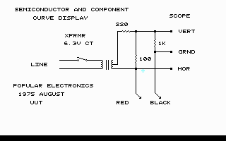
(From: Wern Thiel (wern@zoo.toronto.edu).)
                220
         o-----/\/\-------+---------+-------------o  Vertical Scope Input
                          |         |
                          |         \
           To the 3 V     |         / 1 K
           winding of a   |         \
           6 V center     /         /
           tapped power   \ 100     |
           transformer    /         o-------------o  Ground
                          \         |
                          |         o
                          |  Red component test lead
                          |
                          |  Black component test lead
                          |         o
                          |         |
         o----------------+---------+-------------o Horizontal Scope Input
In the August 1975 issue of Popular Electronics author Lou Garner wrote in a
story called "A simple On-Board Tester" about this fairly simple piece of test
equipment.
The device can be used with any type of oscilloscope and consists of a 6 volt filament transformer, three 1/4 watt resistors and two test probes. Half of the filament voltage is applied to a voltage divider consisting of 220 ohm and 100 ohm resistors, yielding 1 volt ac on top of the 1 K ohm resistor. This voltage can be applied to any component or combination of components across which the test leads are placed. The current is limited to one milliampere by the 1 K ohm resistor.
The voltage across the probes is connected to the horizontal input of a scope while the voltage across the 1 K ohm resistor as a result of the current through it is connected to the vertical input.
What we see on the scope is a voltage across a component under test versus the current through the component:
Resistors:     Open   Horizontal line.
               10 K   10 degree.
                1 K   45 degree.
                  0   Vertical line.

Capacitor:     .1 uF  Shallow ellipse.
              2.6 uF  Circle.
             50.  uF  Narrow vertical.

Transformer:          Ellipse depending on impedance.

Diodes (Germanium):   Right angle display.

Diodes (Silicon):     Right angle one side longer
                      (any leakage showing less sharp angle).

Transistors:          Test as two diodes (B to E and B to C).

Integrated Circuits:  Input for gates and counters show a certain signature
                        display.

                      Outputs display a different signature.

                      A short will show a vertical line.

                      An open will show a horizontal line
In circuit testing is done with *no* power applied to the equipment under test.
With some experience one is able to test components in and out of circuit and troubleshoot without danger of a damage to components.
For FETs, just leave off the transformer.
(From: Michael Covington (mcovingt@ai.uga.edu).)
Get an old Tektronix 575 (mine cost $25 at a hamfest). That is a transistor curve tracer that goes back to the 1950s and goes up to 200 volts.
It doesn't have FET settings, but you can control the 'base' and 'collector' polarity independently. So what you do is put a 1 K resistor from 'base' to ground, so that you can read milliamps as volts. Then put a positive-going voltage on the 'collector' and a negative-going current into the 'base'.
For tubes, emitter, collector, and base are cathode, plate, and grid, respectively. Naturally you also need a filament supply; I use a lab-type DC supply because it's handy and can't introduce hum.
I also test FETs that way (without the filament supply, of course). Then, emitter, collector, and base become source, drain, and gate respectively.
-- end V2.38 --